Device improvement by source to drain resistance lowering through undersilicidation

a technology of drain resistance and device, applied in the field of semiconductor processing, can solve the problems of unacceptably high reverse-bias diode leakage current, unsatisfactory high power consumption and heat propagation in integrated circuits, and conventional cosi.sub.2 processing is not without disadvantages

Inactive Publication Date: 2000-10-17
ADVANCED MICRO DEVICES INC
View PDF10 Cites 39 Cited by
  • Summary
  • Abstract
  • Description
  • Claims
  • Application Information

AI Technical Summary

Problems solved by technology

The resistances can lead to undesirably high power consumption and heat propagation in integrated circuits.
However, conventional CoSi.sub.2 processing is not without disadvantages.
Depending on their depth, size and number, such filaments can cause unacceptably high reverse-bias diode-leakage currents.
Moreover, placing depth constraints on pn junction depth represents a real impediment to transistor geometry scaling.
Another disadvantage of conventional silicide processing is a less than optimal reduction in the source-to-drain resistance in field effect transistors, particularly those embodying lightly doped drain ("LDD") structures.
Although source-to-drain resistan

Method used


Image

  • Device improvement by source to drain resistance lowering through undersilicidation
  • Device improvement by source to drain resistance lowering through undersilicidation
  • Device improvement by source to drain resistance lowering through undersilicidation

Examples


Embodiment Construction

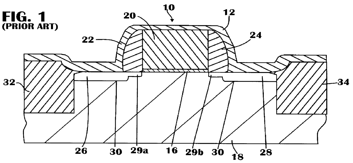
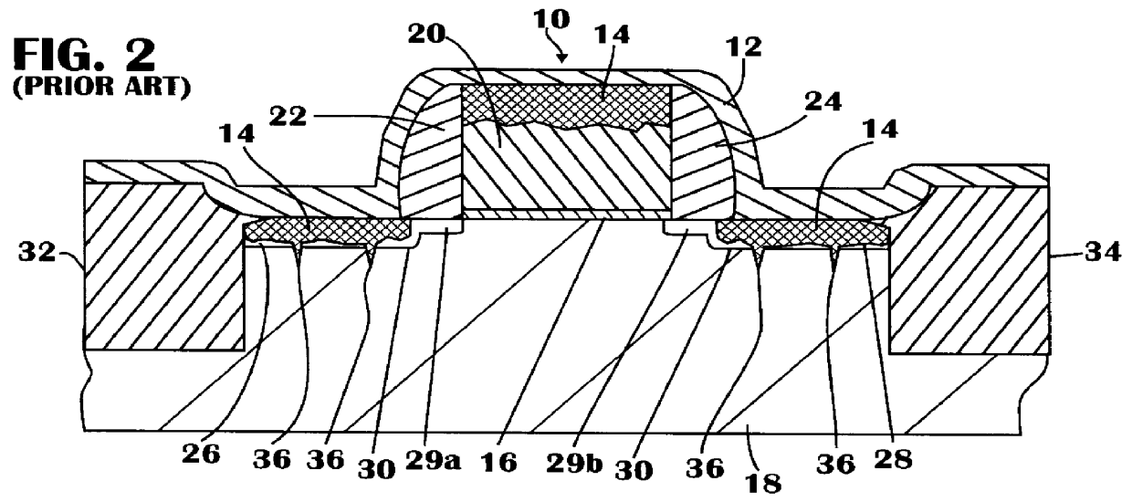
In the drawings described below, reference numerals are generally repeated where identical elements appear in more than one figure. FIGS. 1 and 2 are highly magnified cross-sectional views of a conventional field effect transistor 10. FIG. 1 depicts deposition of a cobalt layer 12 on the transistor 10 while FIG. 2 depicts subsequent thermal silicide reaction to establish a cobalt silicide layer 14. The transistor 10 includes a gate dielectric layer 16 fabricated on a semiconductor substrate 18 and a gate electrode 20 is positioned on the gate dielectric layer 16. The gate dielectric layer 16 and the gate 20 are bracketed by a pair of dielectric sidewall spacers 22 and 24. Source / drain regions 26 and 28 are formed in the substrate 18. The source / drain regions 26 and 28 are provided with respective LDD structures 29a and 29b. The pn junctions for the source / drain regions 26 and 28 are commonly designated 30. The transistor 10 is electrically isolated from various other structures on t...


PUM


Abstract

Various methods of fabricating a silicide layer, and devices incorporating the same are provided. In one aspect, a method of fabricating a silicide layer on a substrate is provided. The method includes the steps of damaging the crystal structure of a portion of the substrate positioned beneath the spacer and depositing a layer of metal on the substrate. The metal layer and the substrate are heated to react the metal with the substrate and form the silicide layer, whereby a portion of the silicide layer extends laterally beneath the spacer. Any unreacted metal is removed. The method enables fabrication of silicide layers with substantial lateral encroachment into LDD structures, resulting in lower possible source-to-drain resistance and enhanced performance for transistors.

Description

1. Field of the InventionThis invention relates generally to semiconductor processing, and more particularly, to a method of fabricating a silicide layer on a substrate with under-spacer penetration.2. Description of the Related ArtA typical field effect transistor implemented in silicon consists of a source and a drain formed in a silicon substrate, and separated laterally to define a channel region in the substrate. A gate electrode composed of a conducting material, such as aluminum or polysilicon, is disposed over the channel region and designed to emit an electric field into the channel region. Changes in the electric field emitted by the gate electrode enable, or alternatively, disable the flow of current between the source and the drain.In a conventional process flow for forming a typical field effect transistor, a gate oxide layer is grown on a lightly doped silicon substrate and a layer of polysilicon is deposited on the gate oxide layer. The polysilicon and the gate oxide ...

Claims


Application Information

Patent Timeline
IPC IPC(8): H01L21/28H01L21/265H01L21/285H01L21/02H01L21/336
CPCH01L21/26586H01L21/28052H01L29/6659H01L29/665H01L21/28518
Inventor HORSTMANN, MANFREDWIECZOREK, KARSTENHAUSE, FREDERICK N.
Owner ADVANCED MICRO DEVICES INC
Why Eureka
Try Eureka