
Semiconductor physical-quantity sensor having a locos oxide film, for sensing a physical quantity such as acceleration, yaw rate, or the like

Inactive Publication Date: 2000-10-24
DENSO CORP
View PDF19 Cites 34 Cited by
  • Summary
  • Abstract
  • Description
  • Claims
  • Application Information

AI Technical Summary

Problems solved by technology

However, in a sensor provided with an electrode of beam structure as shown in FIG. 27A, when static electricity has changed due to acceleration and the voltages V1 and V2 have been caused to change in accompaniment thereto, there exists a problem that, when V1 and V2 become high, an electrical potential differential between the fixed electrodes A41 and A42 and the semiconductor substrate A0 also becomes exceedingly large, and dielectric breakdown occurs between the fixed electrodes A41 and A42 and the semiconductor substrate A0.
A method which forms a sufficiently thick insulation film on the semiconductor substrate surface and forms an anchor portion on this thick insulation film may also be considered as a countermeasure for a problem such as this, but the distance between the fixed portions A41 and A42 and the semiconductor substrate A0 surface is greatly offset with respect to the distance between the movable portion A31 and the semiconductor substrate A0 surface, and a problem occurs wherein the position of the movable portion cannot be controlled with good accuracy.
Additionally, forming a sufficiently thick insulation film on the entirety of the semiconductor substrate surface may also be considered, but a problem occurs wherein a new step to form a hole in this thick insulation film becomes necessary in order to wire the movable portion and the fixed portions.
Namely, there exists a problem that, in a case where voltage applied to the fixed electrodes of both sides has changed during occurrence of acceleration, electrostatic force exerted between the fixed electrodes of both sides and the substrate changes and the fixed electrodes are deformed and displaced with respect to the substrate, the opposing surface area of the movable electrode and the fixed electrodes differs at both sides of the movable electrode, and as a result, the generated electrostatic force differs from the design and acceleration detection of good accuracy cannot be performed.

Method used


Image

  • Semiconductor physical-quantity sensor having a locos oxide film, for sensing a physical quantity such as acceleration, yaw rate, or the like
  • Semiconductor physical-quantity sensor having a locos oxide film, for sensing a physical quantity such as acceleration, yaw rate, or the like
  • Semiconductor physical-quantity sensor having a locos oxide film, for sensing a physical quantity such as acceleration, yaw rate, or the like

Examples


Embodiment Construction

A specific embodiment according to the present invention will be described hereinafter with reference to the drawings.

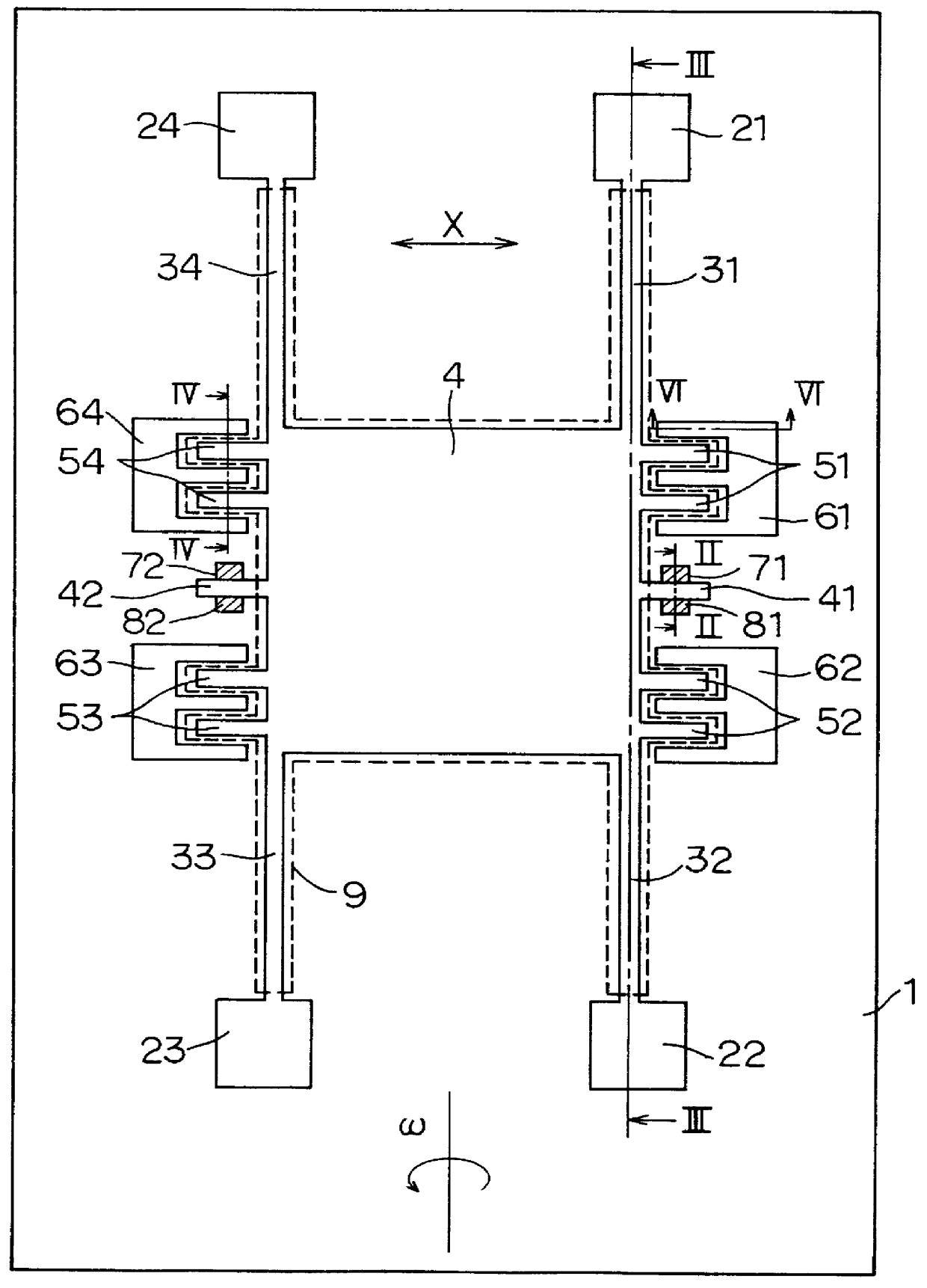
FIG. 1 is a plan view of a yaw-rate sensor according to the present embodiment, which utilizes a transistor for detection of yaw rate.

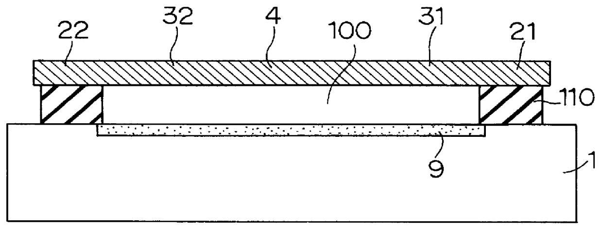
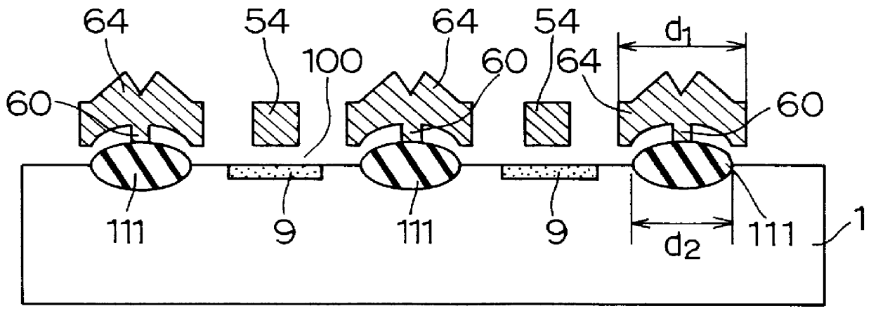
In FIG. 1, a semiconductor substrate 1 is a p-type silicon in the present embodiment. A microstructure suspended in a movable state with respect to the semiconductor substrate exists on the semiconductor substrate 1 surface, and has a structure which will be described hereinafter: a weight (mass) 4 to earn an amount of displacement due to yaw rate; beams 31, 32, 33, and 34 to support the weight 4 in a movable state with respect to the substrate 1; anchor portions 21, 22, 23, and 24 to fix to the substrate 1; movable electrodes 41 and 42 disposed so as to protrude from the weight 4 and which function as a gate in terms of a transistor; and electrodes 51, 52, 53, and 54 for vibration use to impart vibration to the weight 4 and movable el...


PUM


Abstract

The present invention provides a semiconductor physical-quantity sensor which can perform measurement of high accuracy without occurrence of deformation or displacement of a fixed electrode for vibration use even if voltage applied to the fixed electrode for vibration use is changed, and which can increase a dielectric breakdown voltage between the fixed electrode for vibration use and a substrate without varying a thickness of an insulative sacrificial layer or causing sacrificial-layer etching time to be affected. A semiconductor physical-quantity sensor according to the present invention forms an electrode-anchor portion on a sufficiently thick insulation film and causes dielectric breakdown voltage with a semiconductor substrate to be increased. In particular, the sufficiently thick insulation film is given by a LOCOS oxide film formed during sensor detection-circuit fabrication or separation of a diffusion electrode.

Description

This application is based upon and claims the benefit of priority of the prior Japanese Patent Application No. 6-265776 filed on Oct. 28, 1994, the contents of which are incorporated herein by reference.1. Field of the InventionThe present invention relates to a semiconductor physical-quantity sensor employing a semiconductor substrate and a method of fabricating same, and more particularly, to a semiconductor physical-quantity sensor having a beam structure and employing electrostatic force to detect acceleration, yaw rate, or the like, and a method of fabricating same.2. Related ArtsA device indicated in publication SAE910496 exists as an acceleration sensor according to the prior art having a thin-film beam structure. FIG. 27A indicates an entirety of this acceleration sensor.In FIG. 27A, A0 is a Si substrate, A1 is a beam, A2 is a mass, A3 is a movable electrode which forms electrostatic capacitance and performs servo operation, and A4 is a fixed electrode which forms electrosta...

Claims


Application Information

Patent Timeline
IPC IPC(8): G01P15/13G01C19/56G01P15/097G01P15/08G01P15/10G01P15/12G01L1/14B81B3/00G01C19/5719G01P15/00G01P15/125H01L29/84
CPCG01C19/5719G01P15/097G01P15/131G01P15/124G01P2015/0814
Inventor TAKEUCHI, YUKIHIROYAMAMOTO, TOSHIMASAHATTORI, TADASHI
Owner DENSO CORP
Learn More