Liquid crystal display device and manufacturing method for same

a liquid crystal display and manufacturing method technology, applied in non-linear optics, identification means, instruments, etc., can solve problems such as faulty behavior, potential difference between tft substrate and color filter substrate, and electrical charg

Inactive Publication Date: 2000-11-14
NEC LCD TECH CORP
View PDF7 Cites 82 Cited by
  • Summary
  • Abstract
  • Description
  • Claims
  • Application Information

AI Technical Summary

Problems solved by technology

However, along with a large viewing angle, there is a tendency for the liquid crystal cell to accumulate static electricity externally applied, thereby becoming electrically charged.
Therefore, if the surface of the polarizer on the color filter side is touched with the hand, the static electricity of the hand is picked up and passed via the color filter polarizer to the color filter glass substrate, resulting in a potential difference developing between the TFT substrate and the color filter substrate.
The liquid crystal molecules, in response to this potential difference, exhibit faulty behavior and charging occurs.
With this method, however, there are drawbacks, these being (1) a great increase in cost caused by the use of the sputtering method, (2) the occurrence of a loss of the ITO film because of the concentrated discharge current during ESD (electric static damage) testing, because of the excessively low resistance value of the ITO (sheet resistance is approximately 500 .OMEGA. / .quadrature.
This method, however, has the drawbacks of (1) a great increase in cost caused by the use of the sputtering method, the same as the above-noted method of solution, and (2) difficulty in removing the adhesive glue that remains on the ITO film 27 when the polarizer is peeled away.
With this method, however, all that is done is to make the adhesive electrically conductive, and there is no discription with regard to the resistance value, so that there remained the problem of not being able to prevent the loss of the electrically conductive layer when performing ESD testing.
In doing this, if the conductivity is higher than indicated above, there will be a local concentration of discharge current at a probe used in an ESD test, thereby resulting in damage by local burning of the conductive layer of the polarizer.

Method used


Image

  • Liquid crystal display device and manufacturing method for same
  • Liquid crystal display device and manufacturing method for same
  • Liquid crystal display device and manufacturing method for same

Examples


Embodiment Construction

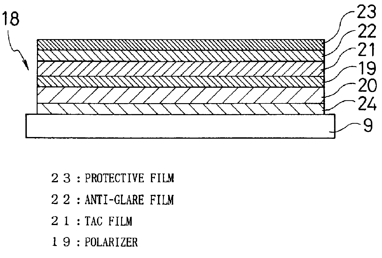
Electrically conductive inorganic metallic particles such as ITO (indium tin oxide), ZnO.sub.2, or Sn.sub.2 O.sub.3 are dispersed into and held by an acrylic resin to form an electrically conductive adhesive material 24. The diameter of these electrically conductive inorganic metallic particles are smaller than the SiO.sub.2 (silicon oxide) particles used in the anti-glare layer 22, this being 2 .mu.m or less and desirably set in the range from 0.02 to 2 .mu.m, the weight ratio of (electrically conductive inorganic metallic particles) / (acrylic resin) being 50% to 80%. By controlling the weight ratio, the resistance value of the electrically conductive adhesive material 24 is established in the range from 1.times.10.sup.3 to 1.times.10.sup.6 .OMEGA. / .quadrature..

The electrically conductive adhesive material 24, which contains these inorganic materials, is applied to the bottom surface of the TAC film 20, which is the base film, using a spin-coat method, a dip-coat method, or a bar-co...


PUM

PropertyMeasurementUnit
diameteraaaaaaaaaa
temperatureaaaaaaaaaa
resistanceaaaaaaaaaa

Abstract

In a liquid crystal display device in which a polarizer is adhered to a transparent glass substrate via an adhesive material, electrically conductive particles are dispersed into and held by an acrylic resin, and the ratio by weight of the electrically conductive particles to the acrylic resin is adjusted to fall in the range from 50% to 80%, so that the resistance value of the adhesive material is in the range from 1x10³ to 1x10⁶ OMEGA / &squ& .

Description

1. Field of the InventionThe present invention relates to a liquid crystal display device and a manufacturing method for a liquid crystal display device, and more specifically to a transverse-field type of liquid crystal display in which display abnormalities caused by static electricity and the like are prevented.2. Background of the InventionA method of driving a liquid crystal display device that controls the liquid crystal by means of a transverse field is indicated, for example, in the Japanese Unexamined Patent Publication (KOKAI) No. 6-160878. Because a feature of a liquid crystal display of this type is that an electrical field is applied in a direction that is parallel to the surface of the liquid crystal cell, the change in the transmissivity of the liquid crystal cell that occurs when the liquid crystal molecules within the liquid crystal cell surface are twisted being used to make a display, in a liquid crystal display device that includes this liquid crystal cell, it is...

Claims


Application Information

Patent Timeline
Patent Type & Authority Patents(United States)
IPC IPC(8): G02F1/13G02F1/1335G02F1/1343G02F1/1333G09F9/35
CPCG02F1/133528G02F1/134363G02F1/1335
Inventor OKAMOTO, MAMORU
Owner NEC LCD TECH CORP
Why Eureka
Try Eureka