MOS type image sensor

a solid-state image and sensor technology, applied in the field of solid-state image sensors, can solve the problems of large power consumption of prior art, hardly installed ccds on the chip, and incongruous techniques with fine-element technology,

Inactive Publication Date: 2000-11-21
NORTH PLATE SEMICON LLC
View PDF4 Cites 110 Cited by
  • Summary
  • Abstract
  • Description
  • Claims
  • Application Information

AI Technical Summary

Problems solved by technology

Then the prior art consumes large power and further has a problem that the CCDs are hardly installed on a chip.
This technique, however, contradicts fine element technology and has some limitations.

Method used


Image

  • MOS type image sensor
  • MOS type image sensor
  • MOS type image sensor

Examples


first embodiment

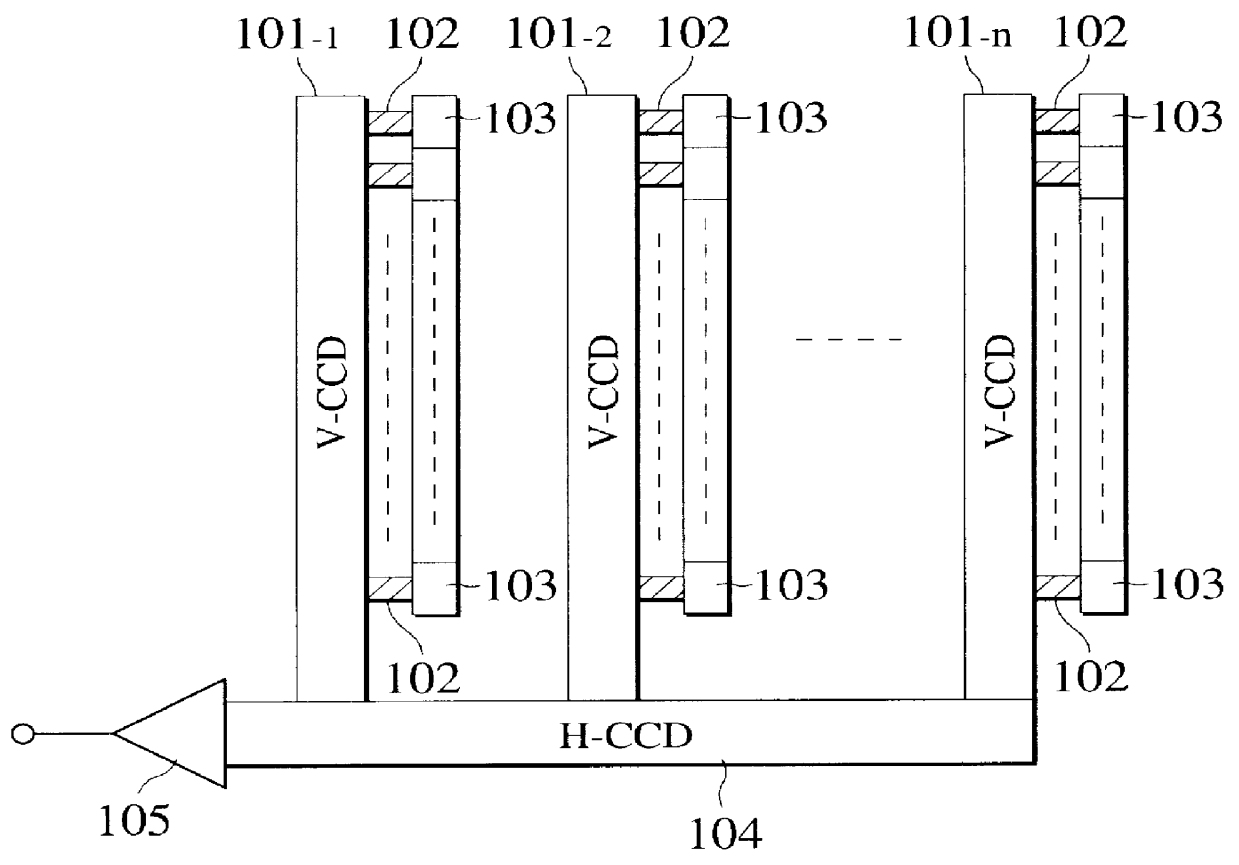
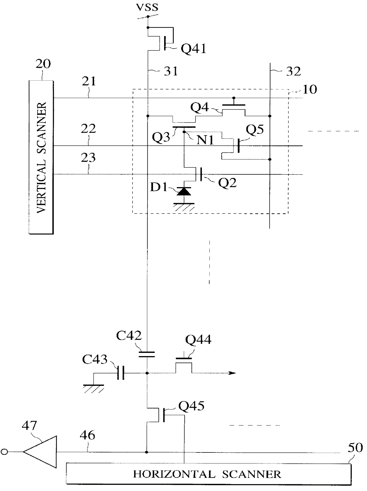
FIG. 3 is a circuit diagram showing an essential part of a MOS type image sensor according to the first embodiment of the present invention. For the sake of simplicity of explanation, only a line of the MOS type image sensor is shown.

The MOS type image sensor consists of an image area and a peripheral circuitry area for driving the image area. The image area consists of pixels 10 that are arranged in a matrix form. Each of the pixels 10 has a photodiode D1 for converting light into carriers, or electron hole pairs. The photodiode D1 is connected to a read MOSFET Q2 that has a specific structure, being characteristic to the first embodiment. The read MOSFET Q2 serves as a transfer gate to read signal charge from the photodiode D1 and transfer the same to a charge detection node N1. The node N1 is connected to a gate electrode of an amplification MOSFET Q3. The amplification MOSFET Q3 is arranged between and connected to a vertical signal line (output signal line) 31 and a row selecti...

second embodiment

FIG. 10 is a plan view showing an essential part of a pixel of a MOS type image sensor according to a second embodiment of the present invention. A circuit diagram of this embodiment is the same as FIG. 3.

In each pixel of the MOS type image sensor of the second embodiment, a vertical signal line (output signal line) 31 and a drain line (power supply line) 32 run vertically. These lines 31 and 32 are made of metal wires. Control signal lines 21, 22, and 23 run orthogonally to the lines 31 and 32. The lines 21 to 23 are made of doped polysilicon wires. The lines 21 to 23 may be made of refractory metal such as W, Ti, and Mo, or silicide thereof such as WSi.sub.2, TiSi.sub.2, and MoSi.sub.2, or polycide employing the silicide. The line 23 is a read line for transmitting a read signal, the line 22 is a reset line for transmitting a reset signal, and the line 21 is a row selection line for transmitting an address (row) selection signal. Unlike the arrangement of FIG. 4, the read line 23 ...

third embodiment

FIG. 14 is a sectional view showing a read MOSFET Q2 and reset MOSFET Q5 of a MOS type image sensor according to a third embodiment of the present invention. A circuit diagram of an essential part of the MOS type image sensor of the third embodiment is the same as FIG. 3, and a plan view thereof is the same as FIGS. 4 and 10. The MOS type image sensor of the third embodiment will be explained on assumptions that design rules with gate length l.sub.0 =0.6 .mu.m are used, MOSFETs are formed in an image area and peripheral circuitry area, and the impurity concentration of p-well regions of the peripheral circuitry area is 2.times.10.sup.17 cm.sup.-3.

The sectional view of FIG. 14 corresponds to one taken along the line V--V of FIG. 4 or the line XI--XI of FIG. 10. At a principal surface of a p-substrate 60, a field oxide film 61 is disposed to isolate an active area from other active areas. At the principal surface of and in the p-substrate 60 disposed in the active area, a p.sup.- -wel...


PUM


Abstract

A MOS type image sensor has an image area that consists of a matrix of pixels and a peripheral circuitry area that drives the image area. To make the MOS type image sensor finer, each of the pixels consists of a second p-well region having a lower impurity concentration than a first p-well region disposed in the peripheral circuitry area; a photodiode having a first main electrode region made of the second p-well region and a second main electrode region formed as a first n-diffusion layer disposed at the surface of the second p-well region; a read transistor having a first main electrode region made of the first n-diffusion layer, a second main electrode region formed as a second n-diffusion layer disposed at the surface of the second p-well region, a gate insulation film disposed on the surface of the second p-well region between the first and second n-diffusion layers, and a gate electrode disposed on the gate insulation film and connected to a read signal line; and an amplification transistor disposed in a third p-well region, having a gate electrode connected to the second main electrode region of the read transistor, a first main electrode region connected to an output signal line, and a second main electrode region. Since the impurity concentration of the second p-well region is low, scaled design rules are employable without causing "white pixels", sensitivity deterioration, signal read voltage increase, or short-channel effect.

Description

1. Field of the InventionThe present invention relates to a solid state image sensor employing an array of pixels, each pixel comprising a photodiode and a plurality of insulated gate transistors such as MOSFETs.2. Description of the Related ArtThere are various solid state image sensors that employ semiconductor devices such as solid state charge-coupled devices (CCDs). The CCD image converters have an interline transfer (IT-CCD), a frame transfer (FT-CCD), charge primitive device (CPD), a photoconductive layer on solid scanner (PLOSS) and other structures. Among them, the interline transfer CCD architecture arranges transfer CCDs between photodiodes.FIG. 1 shows an example of the interline transfer CCD image sensor according to a prior art. In FIG. 1, photodiodes 103 simultaneously transfer accumulated charge to vertical CCDs (V-CCD) 101-1 to 101-n, which transfer the charge of each line of the photodiodes 103 to a horizontal CCD (H-CCD) 104. The horizontal CCD 104 serially transm...

Claims


Application Information

Patent Timeline
Patent Type & Authority Patents(United States)
IPC IPC(8): H01L27/146H04N5/335H04N5/341H04N5/367H04N5/369H04N5/374H04N5/3745
CPCH01L27/14609H04N5/35518H01L27/14643H01L27/14623H04N25/573
Inventor SASAKI, MICHIO
Owner NORTH PLATE SEMICON LLC
Why Eureka
Try Eureka