Method for fabricating a flash memory

a technology of flash memory and fabrication method, which is applied in the direction of semiconductor devices, basic electric elements, electrical appliances, etc., can solve the problems of too small dimension, limited cell density, and small overlap area between floating gate and control gate of flash memory

Inactive Publication Date: 2000-11-28
UNITED MICROELECTRONICS CORP
View PDF3 Cites 70 Cited by
  • Summary
  • Abstract
  • Description
  • Claims
  • Application Information

AI Technical Summary

Benefits of technology

In accordance with the foregoing and other objectives of the present invention, an improved method for fabricating a flash memory is provided. The improved method includes sequentially forming a tunneling oxide layer, a polysilicon layer, and a silicon nitride layer on a semiconductor substrate. Patterning the silicon nitride layer, polysilicon layer, the tunneling oxide layer, and the substrate forms a shallow trench in the substrate. A liner oxide layer is formed on each side wall of the trench, the tunneling oxide layer, and the polysilicon layer. A shallow trench isolation (STI) structure is formed to fill the trench up the silicon nitride layer. The silicon nitride layer is removed to expose the polysilicon layer and a portion of each sidewall of the STI structure, in which the polysilicon is to be further simultaneously patterned later to form a floating gate. A polysilicon spacer is formed on each exposed sidewall of the STI structure. The polysilicon spacer provides more overlapping area between a control gate and a floating gate. An upper portion of the STI structure is removed to fully expose the polysilicon spacer except its bottom on the polysilicon layer and a portion of each sidewall of the polysilicon layer. The exposed portion of each sidewall of the polysilicon further provides more overlapping area. As a result, the coupling ratio is maintained sufficiently large. A conformal dielectric layer and a top polysilicon layer are formed over the substrate. The top polysilicon layer, the dielectric layer, and the polysilicon layer are patterned to form a strip control gate, which covers the floating gate, that is a remaining portion of the polysilicon layer on the tunneling oxide layer. An interchangeable source / drain region is formed in the substrate at active area at each side of the floating gate.

Problems solved by technology

This causes the cell density is limited also.
However, in this manner, an overlapping area between a floating gate and a control gate of the flash memory is accordingly small.
All above problems are induced by a less coupling ratio, which further results from a too small dimension.

Method used


Image

  • Method for fabricating a flash memory
  • Method for fabricating a flash memory
  • Method for fabricating a flash memory

Examples


Embodiment Construction

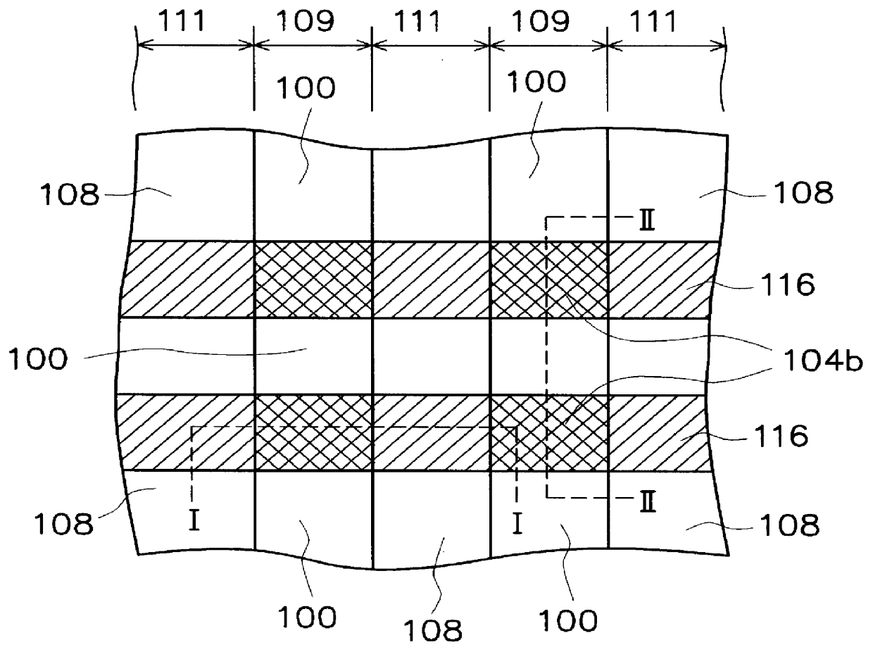
FIG. 1 is a top view of a portion of a substrate, schematically illustrating a structure of a flash memory with a non-AND gate (NAND) structure, according a preferred embodiment of the invention. In FIG. 1, a shallow trench 108 is formed in a semiconductor substrate 100. An active area 109 is simultaneously defined. The shallow trench 108 is filled with insulating material, such as oxide, to form a shallow trench isolation (STI) structure 11. A detail structure is described in FIGS. 2A-2H.

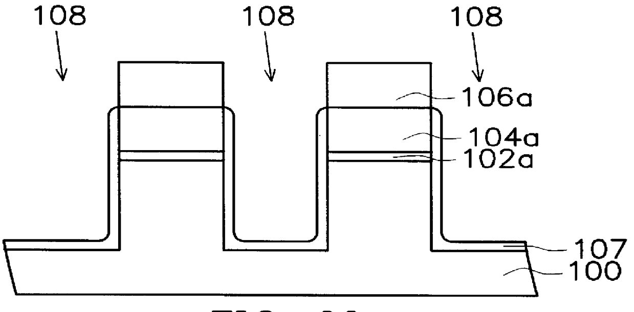
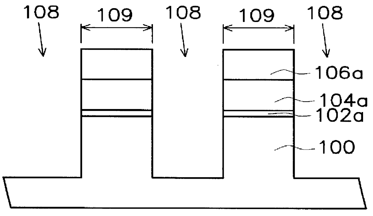
FIGS. 2A-2H are cross-sectional views of a portion of the substrate taken along a line I--I in FIG. 1, schematically illustrating a fabrication process to form a flash memory, according to a preferred embodiment of the invention. In FIG. 2A, there is a semiconductor substrate 100. A tunneling oxide layer 102 is formed on the substrate 100 by, for example, thermal oxidization. A polysilicon layer 104 is formed on the tunneling oxide layer 102 by, for example, chemical vapor deposition (CVD). A mask ...


PUM

PropertyMeasurementUnit
insulatingaaaaaaaaaa
densityaaaaaaaaaa
memory cell densityaaaaaaaaaa

Abstract

A method for fabricating a flash memory is provided. The method contains sequentially forming a tunneling oxide layer, a polysilicon layer, and a silicon nitride layer on a semiconductor substrate. Patterning the silicon nitride layer, polysilicon layer, the tunneling oxide layer, and the substrate forms a trench in the substrate. A shallow trench isolation (STI) structure is formed to fill the trench up the silicon nitride layer. The silicon nitride layer is removed to expose the polysilicon layer and a portion of each sidewall of the STI structure. A polysilicon spacer is formed on each exposed sidewall of the STI structure. An upper portion of the STI structure is removed so as to expose a portion of each sidewall of the polysilicon layer. The polysilicon layer serves as a floating gate. A conformal dielectric layer and a top polysilicon layer are formed over the substrate. The top polysilicon layer, the dielectric layer, and the polysilicon layer are patterned to form a strip control gate, which covers the floating gate, that is a remaining portion of the polysilicon layer on the tunneling oxide layer.

Description

This application claims the priority benefit of Taiwan application serial no. 87121610, filed Dec. 24, 1998, the full disclosure of which is incorporated herein by reference.1. Field of the InventionThis invention relates to semiconductor fabrication, and more particularly to a method for fabricating a flash memory device with a high memory cell density.2. Description of Related ArtRecently, a flash memory with a high memory cell density has significant applications in various apparatus designs. One main advantage of the flash memory is that each memory cell can be fabricated in a greatly reduced dimension, and fabrication cost is also greatly reduced. In a conventional flash memory, memory cells are isolated by a field oxide (FOX) structure that is formed by local oxidation (LOCOS). The FOX structure has its lower limitation of dimension. This causes the cell density is limited also.Another typical isolation structure is a shallow trench isolation (STI) structure. Since the STI str...

Claims


Application Information

Patent Timeline
Patent Type & Authority Patents(United States)
IPC IPC(8): H01L21/70H01L21/8247
CPCH01L27/11521H10B41/30
Inventor DING, YEN-LINHONG, GARY
Owner UNITED MICROELECTRONICS CORP
Why Eureka
Try Eureka