Metallization of buried contact solar cells

a solar cell and contact technology, applied in the field of metalization, can solve the problem of limited choice of dielectrics

Inactive Publication Date: 2000-12-19
UNISEARCH LTD
View PDF7 Cites 91 Cited by
  • Summary
  • Abstract
  • Description
  • Claims
  • Application Information

AI Technical Summary

Benefits of technology

According to a first aspect, the invention provides a method of processing a semiconductor substrate including the steps of forming one or more grooves in a surface of the substrate, selectively applying dielectric coating to the surface by a technique whic

Problems solved by technology

This has greatly limited the available choice for such dielectrics, particularly when the die

Method used


Image

  • Metallization of buried contact solar cells
  • Metallization of buried contact solar cells
  • Metallization of buried contact solar cells

Examples


Embodiment Construction

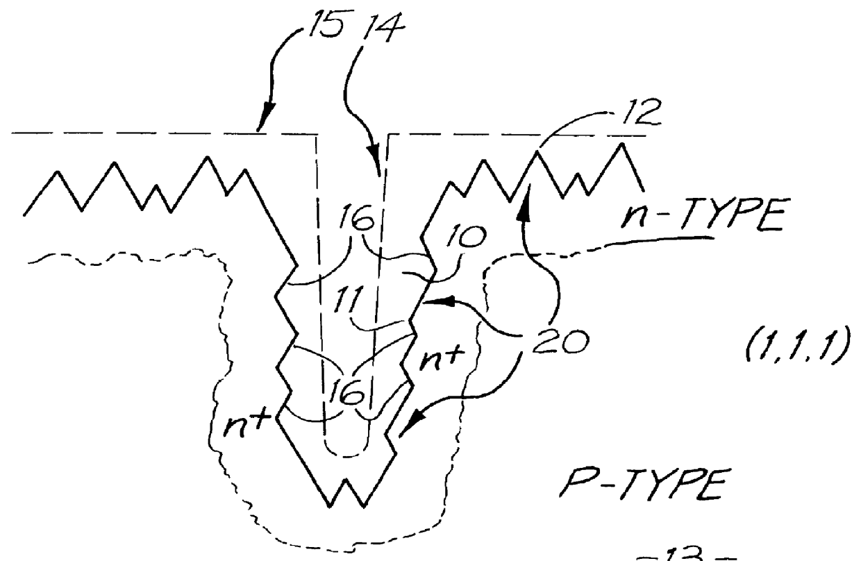
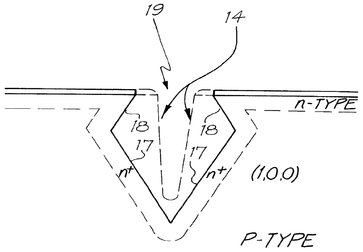
Embodiments of the present invention make use of the geometry of the groove to allow a dielectric layer to be deposited after the groove formation in a way that ensures that at least some regions of the grooves have a substantially thinner layer deposited than the entire top surface. These regions of reduced thickness dielectric within the grooves are then prematurely etched by an appropriate chemical (or other) etchant capable of controllable etching away the dielectric layer. The result is that in these regions the silicon surface can be exposed and able to be plated by the metallization while the top surface of the solar cell remains protected by the dielectric material.

In the above process, the entire groove wall and base does not need to be exposed as only localised areas are sufficient to nucleate plating that will then subsequently facilitate filling the majority of the grooves with the metal. There may in fact be advantages to nucleating the plating only from isolated region...


PUM


Abstract

The present invention makes use of geometry of grooves formed in a substrate, to allow a dielectric layer to be deposited with some regions of the grooves having a substantially thinner layer deposited than top surfaces of the substrate. These regions of reduced thickness dielectric within the grooves are then prematurely etched by an appropriate chemical, or other, etchant capable of controllably etching away the dielectric layer, with the result that in these regions the silicon surface can be exposed and plated by a metallization while the top surface remains protected by the dielectric material. The remaining dielectric material can optionally be required to act as an anti-reflective coating. The invention is applicable in making buried contact solar cells.

Description

The achievement of high efficiencies for solar cells on large area substrates is dependent upon achieving narrow line widths and high aspect ratios (ratio of height to width) for the metallization on the surface exposed to sunlight. The buried contact solar cell [S. R. Wenham and M. A. Green, U.S. Pat. Nos. 4,726,850 and 4,748,130] provides a design for the metallization that achieves both fine line widths and high aspect ratios for the metallization while simultaneously being well suited to commercial production. However, previous implementations of the buried contact solar cell metallization scheme have required the deposition or growth of a dielectric or equivalent layer across the top surface of the substrate early in the processing sequence so as to provide masking of the top surface against diffusions, chemical etching, and metal plating. By necessity, this dielectric masking layer has had to be able to withstand the chemical etching and the high temperature processing without...

Claims


Application Information

Patent Timeline
IPC IPC(8): H01L31/0224H01L31/06H01L31/068H01L31/18
CPCH01L31/022425H01L31/1804H01L31/068Y02E10/547H01L31/03529Y02P70/50
Inventor GREEN, MARTIN ANDREWWENHAM, STUART ROSSHONSBERG, CHRISTIANA B
Owner UNISEARCH LTD
Why Eureka
Try Eureka