Method and apparatus for detecting an initialization signal and a command packet error in packetized dynamic random access memories

a dynamic random access and initialization signal technology, applied in the field of packetized dynamic random access memory devices, can solve the problems of sram cache memory, inability to operate at the speed of the processor, and devoted a lot of effort to increase the operating speed of system memory devices

Inactive Publication Date: 2000-12-26
MICRON TECH INC
View PDF8 Cites 53 Cited by
  • Summary
  • Abstract
  • Description
  • Claims
  • Application Information

AI Technical Summary

Benefits of technology

The invention is directed to a method and apparatus for detecting an initialization flag signal in a packetized DRAM. The DRAM is adapted to receive a command packet, a command clock, and either the initialization flag signal or a normal flag signal, which are applied to a flag input terminal of the DRAM. The initialization flag signal is received prior to initialization of the DRAM, and the normal flag signal is received during normal operation of the DRAM. The normal flag signal has a duration that is substantially shorter than, preferably half, the duration of the initialization flag. In accordance with the inventive method and apparatus, the flag input terminal is sampled by a suitable device, such as a plurality of latches or a shift register. The flag input terminal is sampled at a rate that is sufficiently higher than a plurality of samples, preferably at least 4, are taken during the duration of the initialization flag signal. Th

Problems solved by technology

However, the remaining components of the computer system, with the exception of SRAM cache memory, are not capable of operating at the speed of the processor.
Thus, much effort has been devoted to increasing the operating speed of system memory devices.
However, even SDRAMs are typically incapable of operating at the clock speed of currently available processors.
Thus, SDRAMs cannot be connected directly to the processor bus, but instead must interface with the processor bus through a memory controller, bus bridge, or similar device.
The disparity between the operating speed of the processor and the operating speed of SDRAMs continues to limit the speed at which processors may complete operations requiring access to system memory.
One of the problems of conventional DRAMs is their relatively low speed resulting from the time required to precharge and equilibrate circuitry in the DRAM array.
At higher operating speeds, it can become very difficult to ensure that the ICLK signal has the proper timing to accurately latch the command packet and the FLAG signal.
Even if the timing at which the CMDCLK si

Method used


Image

  • Method and apparatus for detecting an initialization signal and a command packet error in packetized dynamic random access memories
  • Method and apparatus for detecting an initialization signal and a command packet error in packetized dynamic random access memories
  • Method and apparatus for detecting an initialization signal and a command packet error in packetized dynamic random access memories

Examples


Embodiment Construction

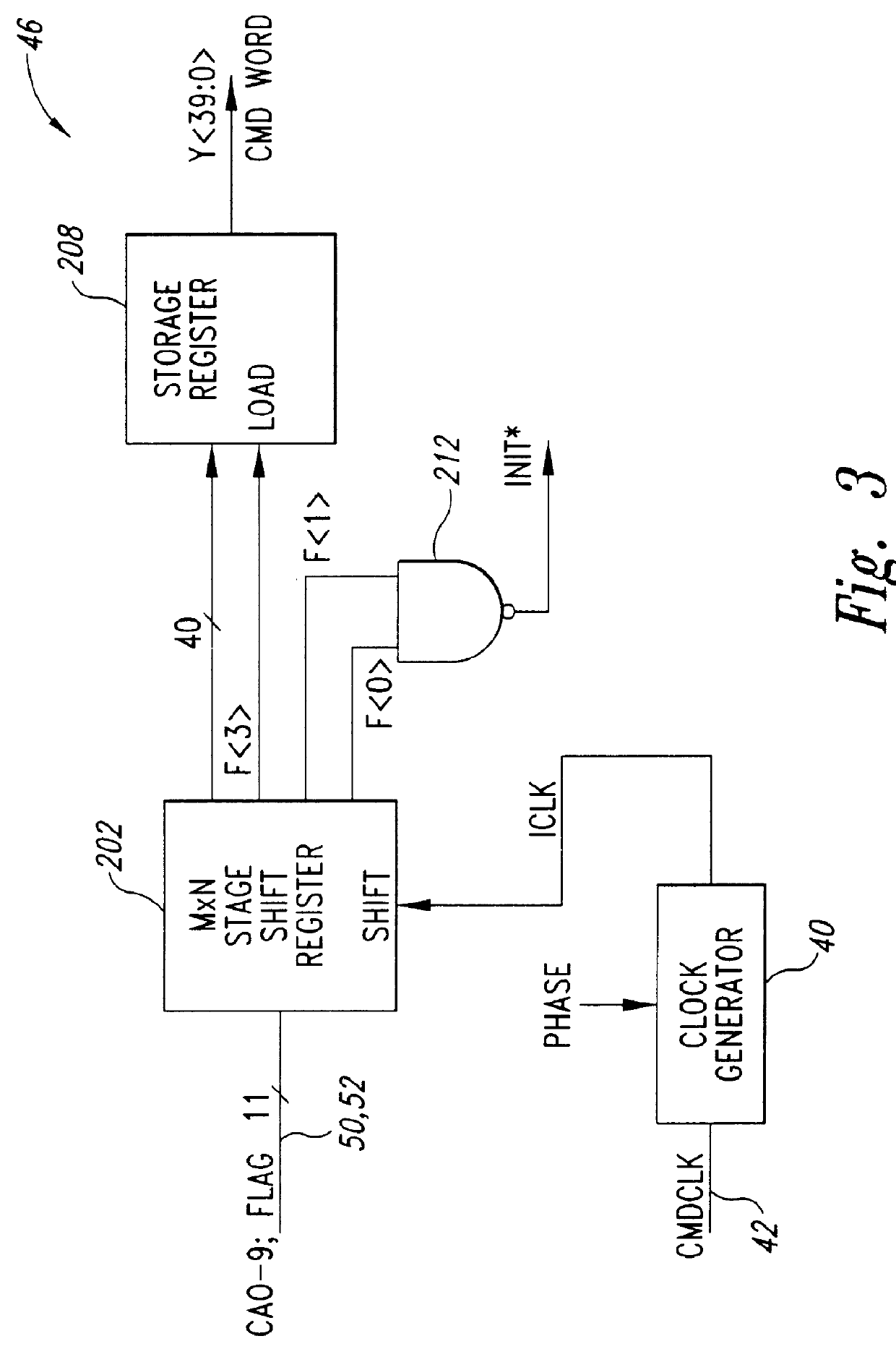
One embodiment of a command buffer 300 in accordance with the invention is illustrated in FIG. 9. The command buffer 300 includes the shift register 202, the storage register 208 and the clock generator circuit 40 from the command buffer 48 of FIG. 3. These components operate in the same manner as explained above unless otherwise noted. Therefore, their operation will not be repeated with reference to FIG. 9. The command buffer 300 does not include the NAND gate 212 of FIG. 3 because the INIT* signal is instead generated by an Initialization Flag Detector 306.

The Initialization Flag Detector 306 receives the FLAG signal and a flag clock signal FCLK. As explained further below, the FCLK signal has a frequency that is higher than the frequency of the internal clock signal ICLK. The FCLK signal is preferably generated from the ICLK signal and is preferably an integer of multiple of the ICLK signal. However, the FCLK signal may be generated independently of the ICLK signal as long as it...


PUM


Abstract

A system for detecting an initialization flag signal and distinguishing it from a normal flag signal having half the duration of the initialization flag signal. The initialization flag detection system may be included in the command buffer of a packetized DRAM that is used in a computer system. In one embodiment, the initialization flag detection system includes a pair of shift registers receiving the flag signal at their respective data inputs. One of the shift registers is clocked by a signal corresponding to an externally applied to command clock signal, while the other shift register is clocked by a quadrature clock signal. Together, the shift registers store a number of samples taken over a duration that is longer than the duration of the normal flag signal. The outputs of the shift registers are applied to a logic circuit, such as a NAND gate, that generates an initialization signal when all of the samples stored in the shift registers correspond to the logic levels of the flag signal. In another embodiment, the initialization flag detection system includes a plurality of latches receiving the flag signals at their data inputs. The latches are clocked by respective strobe signals corresponding to the command clock signal, but having phases that differ from each other. The outputs of the latches are applied to a logic circuit, such as a NAND) gate. Finally, in another embodiment of the invention, the bits of the command packet are sampled along with the flag signal and compared to the samples of the flag signal to detect when a command packet having a predetermined pattern does not correspond to a flag signal having a predetermined pattern.

Description

TECHNICAL FIELDThe present invention relates to packetized dynamic random access memory devices, and more particularly, to a method in apparatus for detecting a signal indicating the start of an initialization procedure that adjusts the timing of an internal clock signal used to strobe the initialization signal and a command packet.BACKGROUND OF THE INVENTIONConventional computer systems include a processor (not shown) coupled to a variety of memory devices, including read-only memories ("ROMs") which traditionally store instructions for the processor, and a system memory to which the processor may write data and from which the processor may read data. The processor may also communicate with an external cache memory, which is generally a static random access memory ("SRAM"). The processor also communicates with input devices, output devices, and data storage devices.Processors generally operate at a relatively high speed. Processors such as the Pentium.RTM. and Pentium II.RTM. micro...

Claims


Application Information

Patent Timeline
IPC IPC(8): G11C7/10G11C7/20G11C7/00
CPCG11C7/20G11C7/1072
Inventor KEETH, BRENTMANNING, TROY A.
Owner MICRON TECH INC
Why Eureka
Try Eureka