In situ method for cleaning silicon surface and forming layer thereon in same chamber

a technology of silicon surface and in situ method, which is applied in the direction of coating, chemical vapor deposition coating, coating, etc., can solve the problems of multiple wafers being handled, the yield of impurities and contaminants is unacceptable, and the yield of semiconductor devices is unacceptabl

Inactive Publication Date: 2001-03-06
APPLIED MATERIALS INC
View PDF15 Cites 87 Cited by
  • Summary
  • Abstract
  • Description
  • Claims
  • Application Information

AI Technical Summary

Problems solved by technology

As device geometries become smaller, for example, using submicron design rules, impurities and contaminants exact an unacceptable toll on semiconductor device per wafer yields.
Unfortunately, however, the use of such prior art chambers also encourages the growth of native oxides and other contaminants.
Handling of multiple wafers, e.g. in a wafer boat, at multiple processing stations during the semiconductor device fabrication process is a particularly acute problem with regard to the formation of native oxides, or the introduction of other impurities to the wafer surfaces.
This problem is exacerbated by the fact that such native oxide forms in a nonuniform manner, i.e., the first wafer in the chamber may grow a thicker layer of native oxide.
Otherwise, such contaminants and impurities present at the interface between the silicon surface of the wafer and the layer formed thereover may interfere with the electrical properties of the integrated circuit structures therein, resulting, for example, in device noise, degraded performance, or even total failure of the integrated circuit structure.
The formation of native oxide and the presence of various contaminants on the silicon surface of a wafer becomes an increasingly serious problem as device geometries become smaller.
Native oxides also present a serious problem, for example in bipolar emitter technology, where a very thin (e.g., 20 Angstroms), but uniform, oxide layer is to be grown on the silicon surface of the wafer; as well as inhibiting effective polysilicon deposition.
That is, very thin and uniform oxide layers as are required, for example, in submicron semiconductor device structures, cannot be predictably produced when random native oxide is already present on the underlying silicon surface.
Rather, an intentionally grown oxide layer over such native oxides will have undesired raised or thick portions at points where native oxides are present on the wafer surface beneath the grown oxide layer.
Additionally, such native oxides may include various contaminants.

Method used


Image

  • In situ method for cleaning silicon surface and forming layer thereon in same chamber
  • In situ method for cleaning silicon surface and forming layer thereon in same chamber
  • In situ method for cleaning silicon surface and forming layer thereon in same chamber

Examples


Embodiment Construction

The present invention is a method for cleaning a silicon surface of a semiconductor wafer in a vacuum chamber within a first temperature range in the presence of hydrogen gas; then cooling the wafer down to a second temperature range; and then forming a layer of either polysilicon or oxide over the cleaned surface within this second temperature range without removing the cleaned wafer from the chamber.

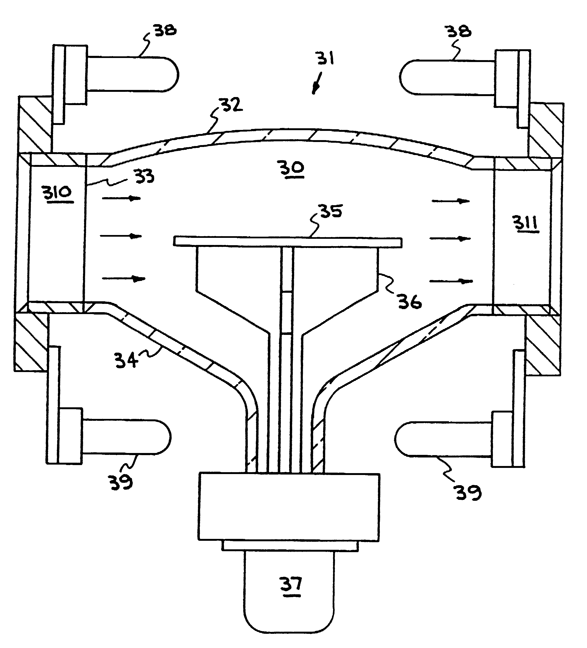
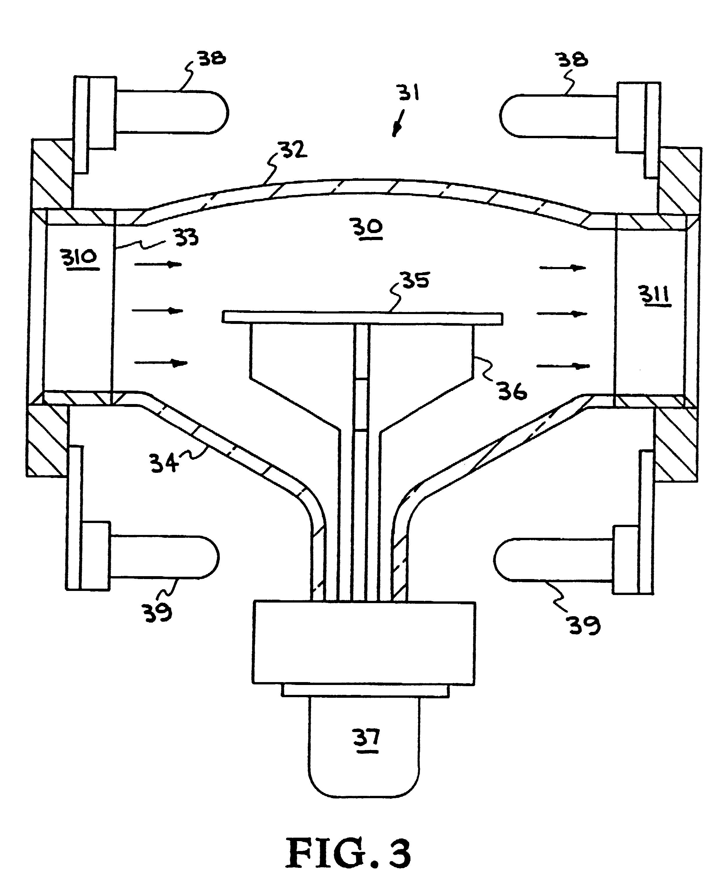
For purpose of illustration, the present process is described with reference to FIG. 3 which illustrates a single wafer reactor 31 which includes a top wall 32, side walls 33, and a bottom wall 34 that define a chamber 30 into which a single semiconductor wafer 35, having a silicon surface, is loaded. Top wall 32 and bottom wall 34 are both substantially transparent to light, at least of infrared frequency, to allow external radiant heating of wafer 35 within chamber 30 as will be described below. Typically, top wall 32 and bottom wall 34 are formed of a high strength, transparent mate...


PUM

PropertyMeasurementUnit
temperatureaaaaaaaaaa
pressureaaaaaaaaaa
pressureaaaaaaaaaa

Abstract

A method is described for cleaning a silicon surface of a semiconductor wafer in a vacuum chamber while radiantly heating said silicon surface to maintain it within a first temperature range in the presence of hydrogen gas; then quickly cooling the wafer down to a second temperature range by reducing the radiant heat; and then forming a layer of either polysilicon or oxide over the cleaned surface within this second temperature range without removing the cleaned wafer from the chamber. By cleaning the wafer and then depositing polysilicon or growing oxide over the cleaned silicon surface in the same vacuum chamber, formation of oxides and other contaminants on the cleaned silicon surface between the cleaning step and the deposition or growth step is inhibited, resulting in a higher quality polysilicon or oxide layer formed over the cleaned silicon surface.

Description

1. Field of the InventionThis invention relates to the fabrication of semiconductor devices. More particularly, this invention relates to a method for cleaning a silicon surface to remove native oxides and other contaminants in situ and then forming a layer, such as a layer of polysilicon or a layer of oxide, over the cleaned silicon surface in the same chamber.2. Description of the Related ArtDuring the fabrication of semiconductor devices on silicon wafers, various structures are formed on a silicon substrate. The quality of the semiconductor device is a function of the accuracy with which these structures are formed, as well as the cleanliness of the environment in which the semiconductor device is processed. As device geometries become smaller, for example, using submicron design rules, impurities and contaminants exact an unacceptable toll on semiconductor device per wafer yields.A critical step during the process of fabricating certain semiconductor devices involves depositing...

Claims


Application Information

Patent Timeline
Patent Type & Authority Patents(United States)
IPC IPC(8): C23C16/02H01L21/285H01L21/02H01L21/316H01L21/306H01L21/205
CPCC23C16/0218H01L21/02046H01L21/02238H01L21/02255H01L21/02301H01L21/02312H01L21/28525H01L21/31612H01L21/31662H01L21/02381H01L21/02532H01L21/0262H01L21/02661Y10S438/906Y10S438/974Y10S148/017
Inventor BEINGLASS, ISRAEL
Owner APPLIED MATERIALS INC
Why Eureka
Try Eureka