Dynamic burn-in test equipment

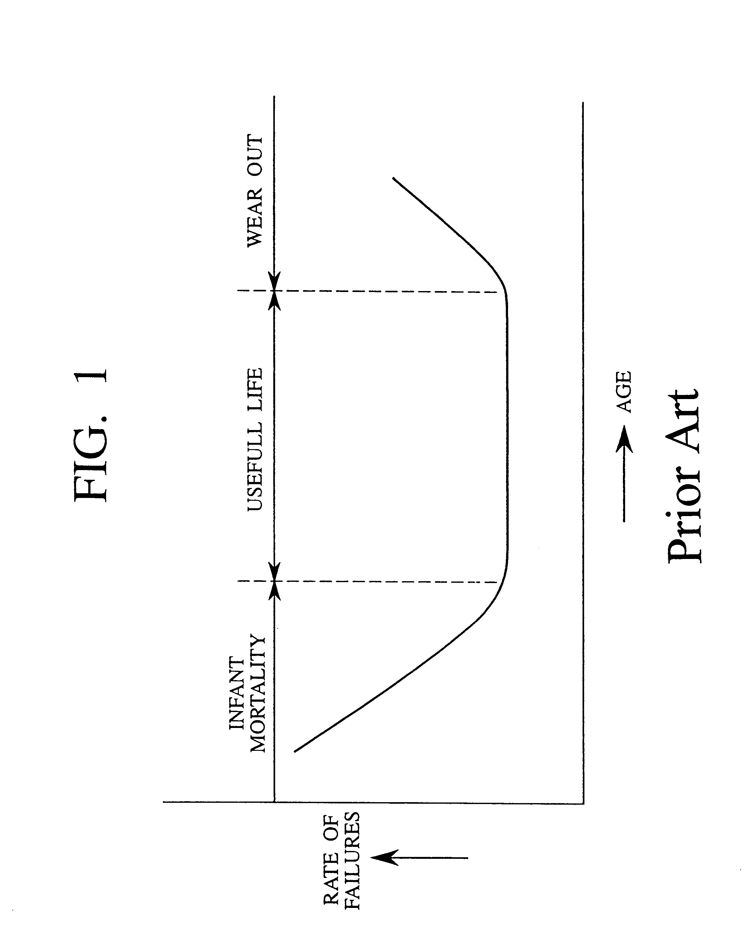
a test equipment and burn-in technology, applied in the direction of individual semiconductor device testing, semiconductor/solid-state device testing/measurement, instruments, etc., can solve the problems of increasing the acceleration the development speed of testing techniques is gradually behind the development speed of semiconductor devices, and the variety of new functions to be added to semiconductor devices

Inactive Publication Date: 2001-04-10
NIPPON SCI
View PDF3 Cites 55 Cited by
  • Summary
  • Abstract
  • Description
  • Claims
  • Application Information

AI Technical Summary

Problems solved by technology

However, the development speed of semiconductor devices acceleratively increases, miscellaneous new functions to be added to the semiconductor devices become varied.
Nowadays, the development speed of the testing technique is gradually behind the development speed of the semiconductor device.
In particular, it has been very difficult to perform a reliability test for multi-pin LSI chips within a short test time and at a low cost.
After the infant mortality failures are culled out, the component settle into a long period of useful life failure, called "over stress failures" or "intrinsic failures" which are caused by high-level stress outside those expected in normal usage.
Finally, wearout failures begin to be significant as normal wear out mechanisms start to take their toll on components that are manufactured within acceptable specifications.
More specifically, a limited lifetime is caused by the presence of any defect.
If the defect is accelerated and increased by the elevated temperature under the test condition, the product is recognized as a defective.
However, an annealing temperature is limited to a predetermined value because good products must not be damaged.
When signals are given to an LSI, or a device under test (DUT) at random, all the internal circuits of the DUT cannot be operated.
However, in a conventional static burn-in technique, the static burn-in testing requires very long test time.
In addition, the burn-in test equipment is expensive, and a running cost is high.
Namely, the failure rate of a large number of DUTs cannot be actually measured because the equipment configuration becomes very complex and because a test time becomes extremely long.
At present, since the number of output pins of an LSI chip tends to increase, the following problem is posed.
That is, it is becoming more and more difficult or impossible that a failure rate of LSI chips is measured in a short test time and with a low cost.
However, when abnormality occurs in the internal circuit of the LSI chip, a difference between the output from the internal circuit and the expected value supplied from driving unit is generated.

Method used


Image

  • Dynamic burn-in test equipment
  • Dynamic burn-in test equipment
  • Dynamic burn-in test equipment

Examples


Embodiment Construction

)

A preferred embodiment of the present invention will be described with reference to the accompanying drawings. It is to be noted that the same or similar reference numerals are applied to the same or similar parts and elements throughout the drawings, and the description of the same or similar parts and elements will be omitted or simplified. Generally and as it is conventional in the representation of instrument, it will be appreciated that the various drawings are not drawn to scale from one figure to another nor inside a given figure. In the following description, numerous specific details are set fourth such as specific circuit, etc. to provide a through understanding of the present invention. However, it will be obvious to those skilled in the art that the present invention may be practiced without such specific details.

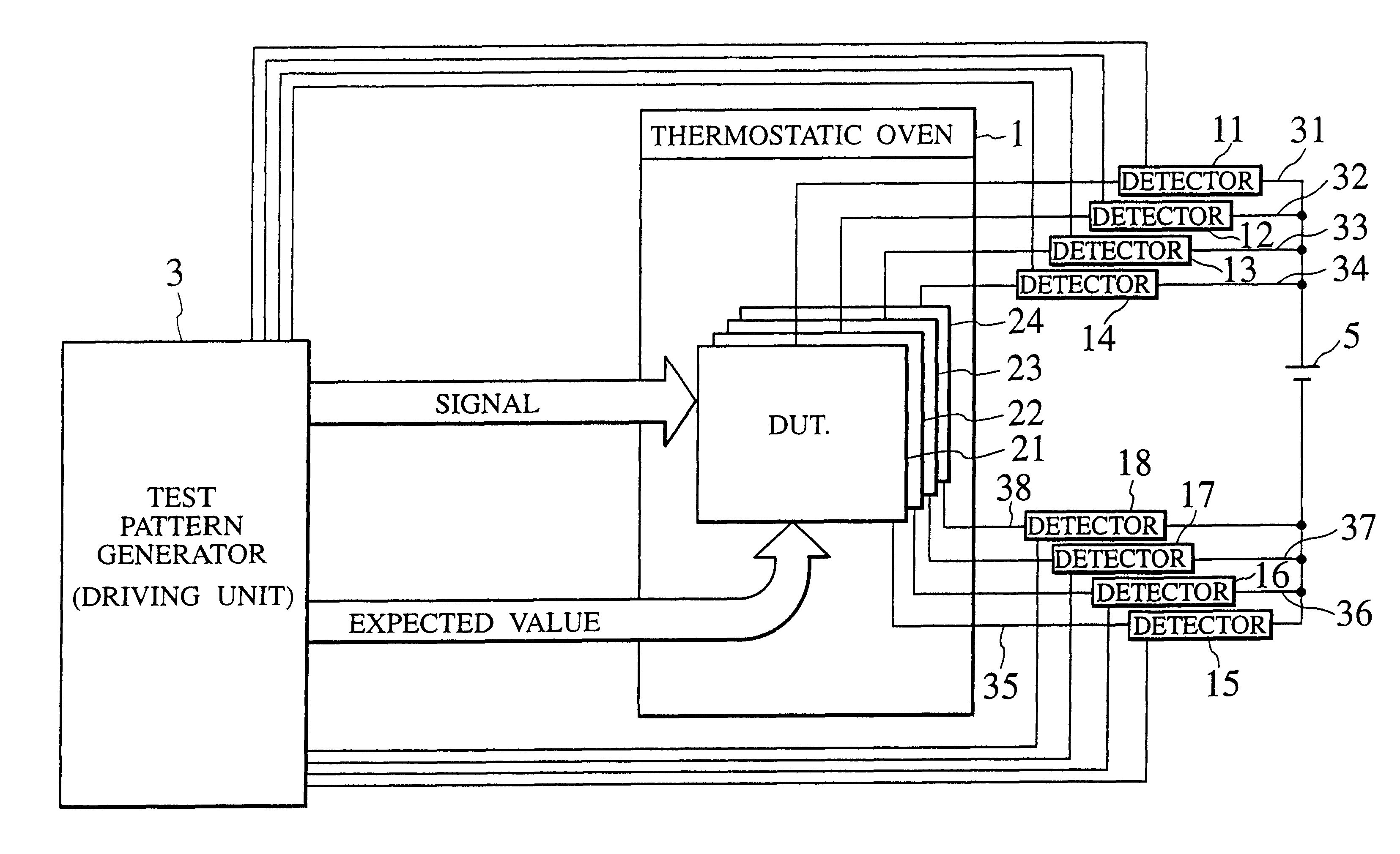
FIG. 5 is a diagram showing the basic configuration of the dynamic burn-in test equipment according to the embodiment of the present invention. More specifical...


PUM


Abstract

There is provided a dynamic burn-in test equipment being capable of testing a large number of multi-pin LSI chips in a short test time and at a low cost. The dynamic burn-in test equipment includes at least a thermostatic oven for storing DUTs, a driving unit for applying the input signal to the input terminal of each DUT to apply a predetermined expected value to the output terminal of each DUT, a power supply for applying a predetermined power supply voltage to each DUT through a higher level power supply line and a lower level power supply line (ground line), and a current detector arranged on at least one of the higher level power supply line and the lower level power supply line (ground line). The dynamic burn-in test equipment monitors a power supply current to detect a failure.

Description

The subject application is related to subject matter disclosed in the Japanese Patent Application No. Hei 11-2080 filed in Jan. 7, 1999 in Japan, to which the subject application claims priority under the Paris Convention and which is incorporated by reference herein.1. Field of the InventionThe present invention relates to a reliability test equipment and a failure rate test equipment. More particularly, the present invention relates to a dynamic burn-in test equipment for testing large scale integration chips (LSI chips) sealed in packages each having a large number of I / O pins. Here, the LSI chips may include very large scale integration chips (VLSI chips), ultra large scale integration chips (ULSI chips) or gigascale integration chips (GSI chips).2. Description of the Related ArtIn recent years, the operation speeds, the memory capacities, and the numbers of bits of semiconductor devices are considerably increasing. As high-speed semiconductor devices, devices having operation f...

Claims


Application Information

Patent Timeline
Patent Type & Authority Patents(United States)
IPC IPC(8): G01R31/28G01R31/26H01L21/66
CPCG01R31/2879
Inventor YOSHIDA, NAOKI
Owner NIPPON SCI
Why Eureka
Try Eureka