Extended range and ultra precision non contact dimensional gauge for ultra thin wafers and work pieces

a non-contact dimensional, ultra-thin wafer technology, applied in the direction of fluid pressure measurement using inductance variation, instruments, mechanical means, etc., can solve the problems of back pressure measurement circuits that are sensitive to regulators, and the system of '661 patent cannot be used for geometrical parameters measurements of ultra-thin wafers with less than 200 microns thickness

Inactive Publication Date: 2001-04-24
MICROSENSE
View PDF20 Cites 23 Cited by
  • Summary
  • Abstract
  • Description
  • Claims
  • Application Information

AI Technical Summary

Problems solved by technology

The back pressure measurement circuits are very sensitive to regulator pressure variations because the output pressure variations appear as common mode noise to the detector.
However, the system of '661 patent cannot be used for measurements of geometrical parameters (for example, the warpage and bow) of ultra-thin wafers with the thickness less than 200 microns.
This is due to the fact that the ultra thin wafer with the thickness less than 200 microns vibrates under the air pressure that is used in the back pressure sensor of '661 patent, thus making it impossible to measure the curvature of an ultra-thin wafer.

Method used


Image

  • Extended range and ultra precision non contact dimensional gauge for ultra thin wafers and work pieces
  • Extended range and ultra precision non contact dimensional gauge for ultra thin wafers and work pieces
  • Extended range and ultra precision non contact dimensional gauge for ultra thin wafers and work pieces

Examples


Embodiment Construction

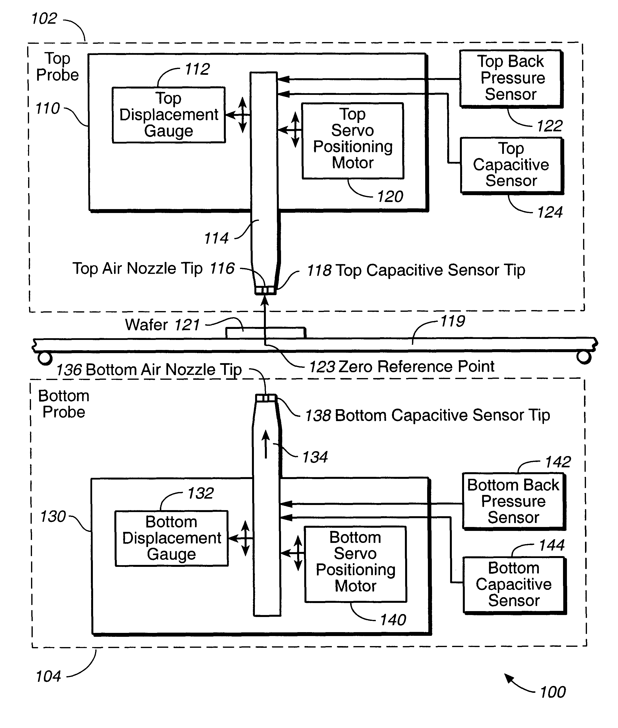
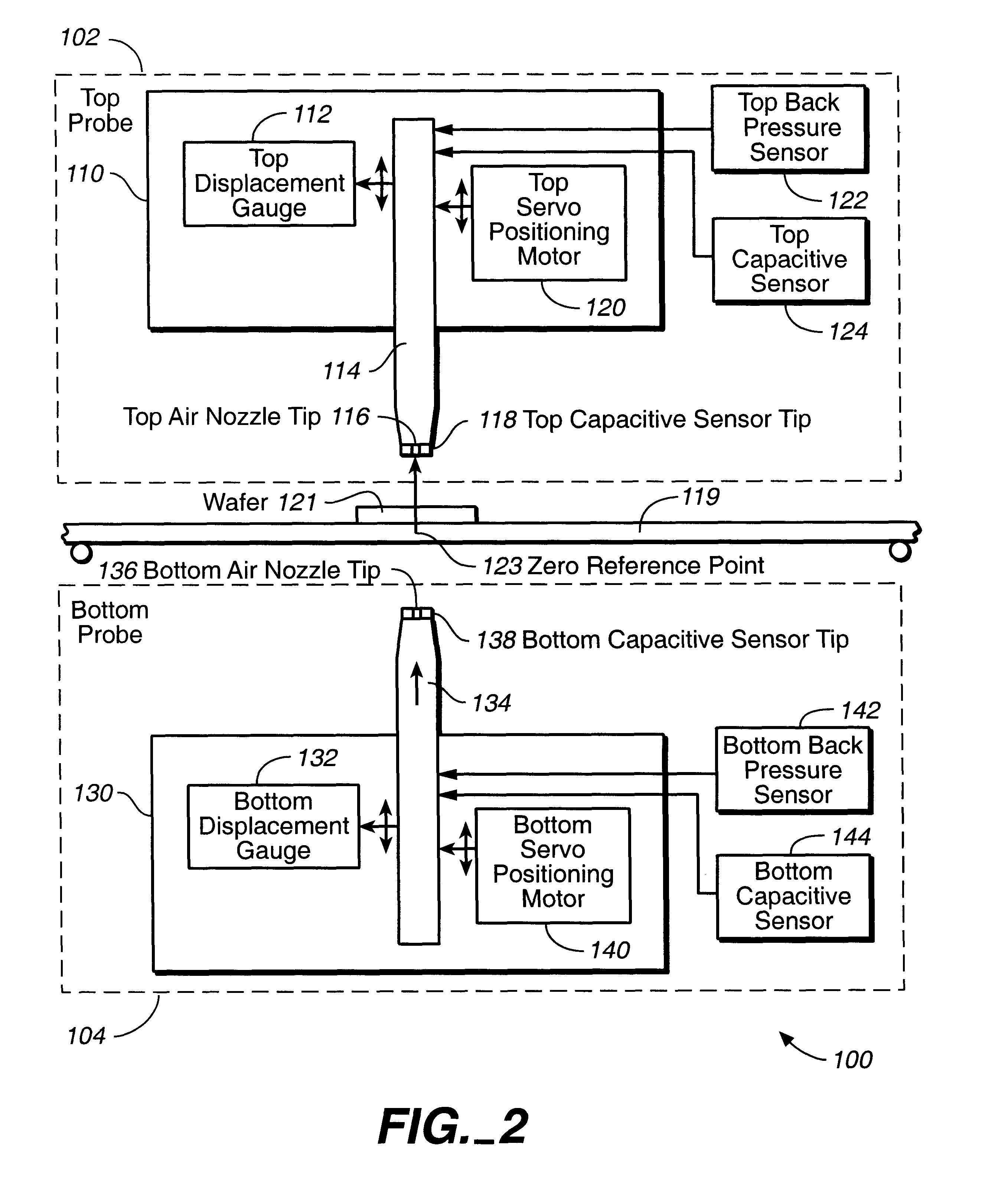
An ultra thin wafer (with thickness less than 200 microns) is not rigid. When placed on the stage and held at 3 points near the edge, due to gravity, a wafer tends to bow in the center. In addition, the stress induced in a wafer through various manufacturing processes tends to give the wafer a specific shape with warpage. Bow and warpage can reach relatively large dimensions (over 1000 microns).

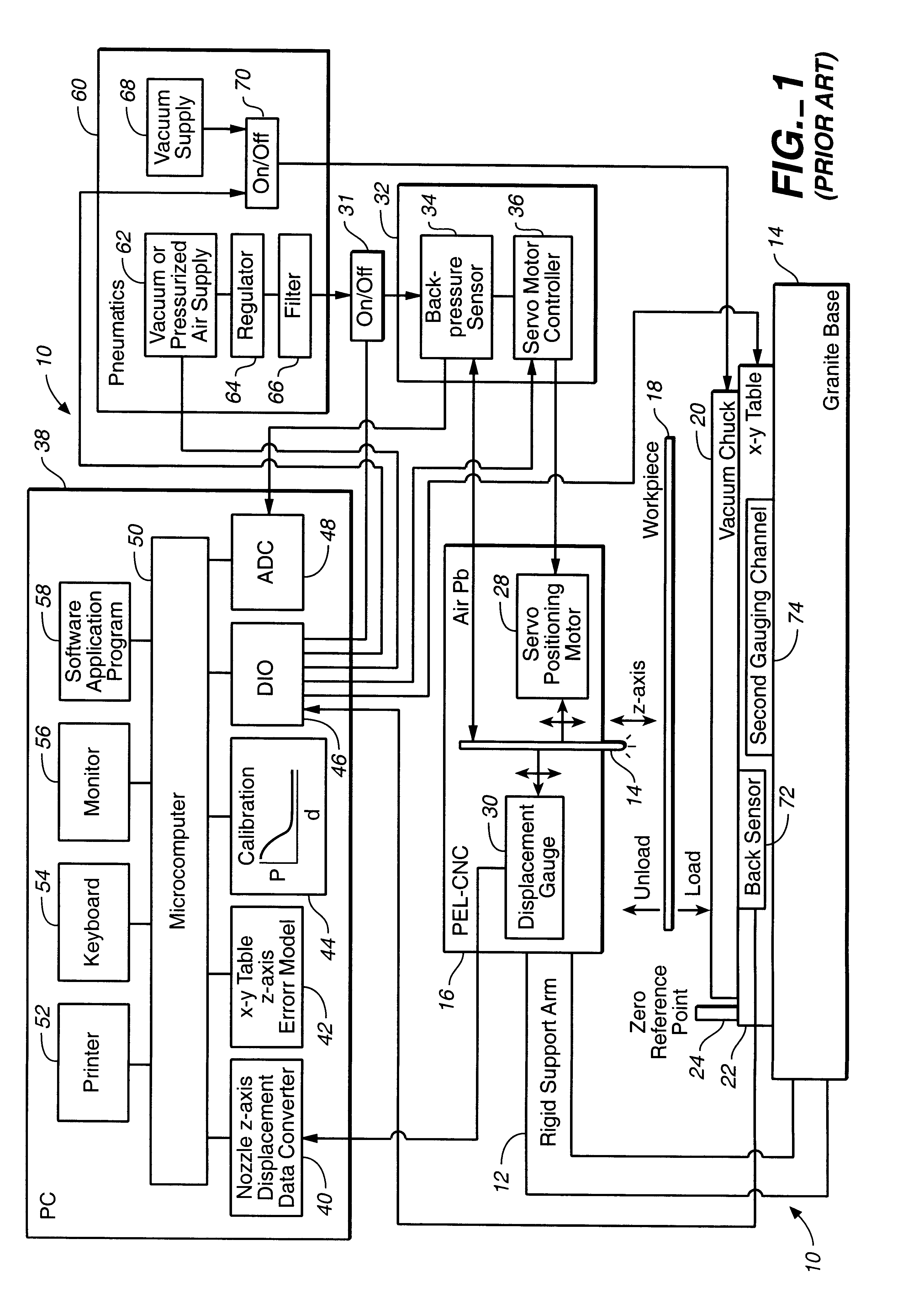
The prior art methods of gauging the geometrical parameters of a wafer, (like thickness, bow, and warpage) have their limitations. Indeed, when using the prior art capacitive sensors for gauging purposes, the capacitive probes have to be maintained fixed and allow only maximum bow and warpage in the range of 500 microns. For such prior art optical methods as laser beam, the wafer surface finish and the wafer's type of material generally created measurement problems. For the prior art air gauging method, air flow tends to induce vibrations on very thin work pieces (or wafers) unless the work p...


PUM

PropertyMeasurementUnit
linear displacement gaugeaaaaaaaaaa
thicknessaaaaaaaaaa

Abstract

A method and a system for measurement the geometrical parameters of ultra thin wafers with the thickness less than 200 microns. The measurement system comprises two measurement channels and a computer. Each measurement channel comprises a motor-positionable probe further comprising a back pressure probe and a capacitive probe. The capacitive probe is substantially cocentric with the back pressure probe. The air back pressure sensor is used to calibrate the capacitive sensor for a given dielectric permittivity of the conductive target, and the capacitive sensor is used to measure thickness, flatness, bow, and warpage of the ultra-thin electrically conductive target.

Description

The current invention is in the field for gauging the thickness of conductive targets, and more specifically, in the field for ultra precision non contact dimensional gauging the geometrical properties of ultra thin conductive wafers.DESCRIPTION OF THE BACKGROUND ARTIn the available art, the non-contact sensing and pneumatic gauging is based on measuring the backpressure of compressed air flow to a nozzle in very close proximity to a workpiece surface. In a prior art conventional pneumatic gauging circuit, the air gap distance between the nozzle outlet and the workpiece surface is estimated by using the back pressure in a chamber through which compressed air is flowing via a restricted orifice. Such back pressure is function of the distance that separates the tip of the nozzle connected to the chamber and the adjacent surface of the workpiece. The supply air pressure to the back pressure circuits is precisely regulated.The back pressure measurement circuits are very sensitive to reg...

Claims


Application Information

Patent Timeline
Patent Type & Authority Patents(United States)
IPC IPC(8): G01B13/00G01B13/06
CPCG01B13/06
Inventor FAUQUE, JACQUES A.
Owner MICROSENSE
Why Eureka
Try Eureka