Erasable and programmable nonvolatile semiconductor memory, semiconductor integrated circuit device having the semiconductor memory and method of manufacturing the semiconductor memory

a non-volatile, semiconductor technology, applied in the direction of digital storage, instruments, transistors, etc., can solve the problems of nand-type eeproms having problems, unable to write or be difficult to write, and read errors

Inactive Publication Date: 2001-04-24
KK TOSHIBA
View PDF8 Cites 30 Cited by
  • Summary
  • Abstract
  • Description
  • Claims
  • Application Information

AI Technical Summary

Problems solved by technology

The ROMs allow to write information into them during manufacturing or after manufacturing, and the information once written therein is completely unable to rewrite or is difficult to rewrite.
However, the NAND-type EEPROMs have some problems.
The threshold-voltage variations reduce a margin in determining whether information read out of a given cell is "0" or "1" and may cause a read error.
During the read operation, the electric field concentration gradually accumulates a charge by injecting electrons from the channel region into a floating gate electrode through a tunnel insulation film, thereby causing soft-writing (erroneous writing).

Method used


Image

  • Erasable and programmable nonvolatile semiconductor memory, semiconductor integrated circuit device having the semiconductor memory and method of manufacturing the semiconductor memory
  • Erasable and programmable nonvolatile semiconductor memory, semiconductor integrated circuit device having the semiconductor memory and method of manufacturing the semiconductor memory
  • Erasable and programmable nonvolatile semiconductor memory, semiconductor integrated circuit device having the semiconductor memory and method of manufacturing the semiconductor memory

Examples


Embodiment Construction

Various embodiments of the present invention will be described with reference to the accompanying drawings. It is to be noted that the same or similar reference numerals are applied to the same or similar parts and elements throughout the drawings, and the description of the same or similar parts and elements will be omitted or simplified.

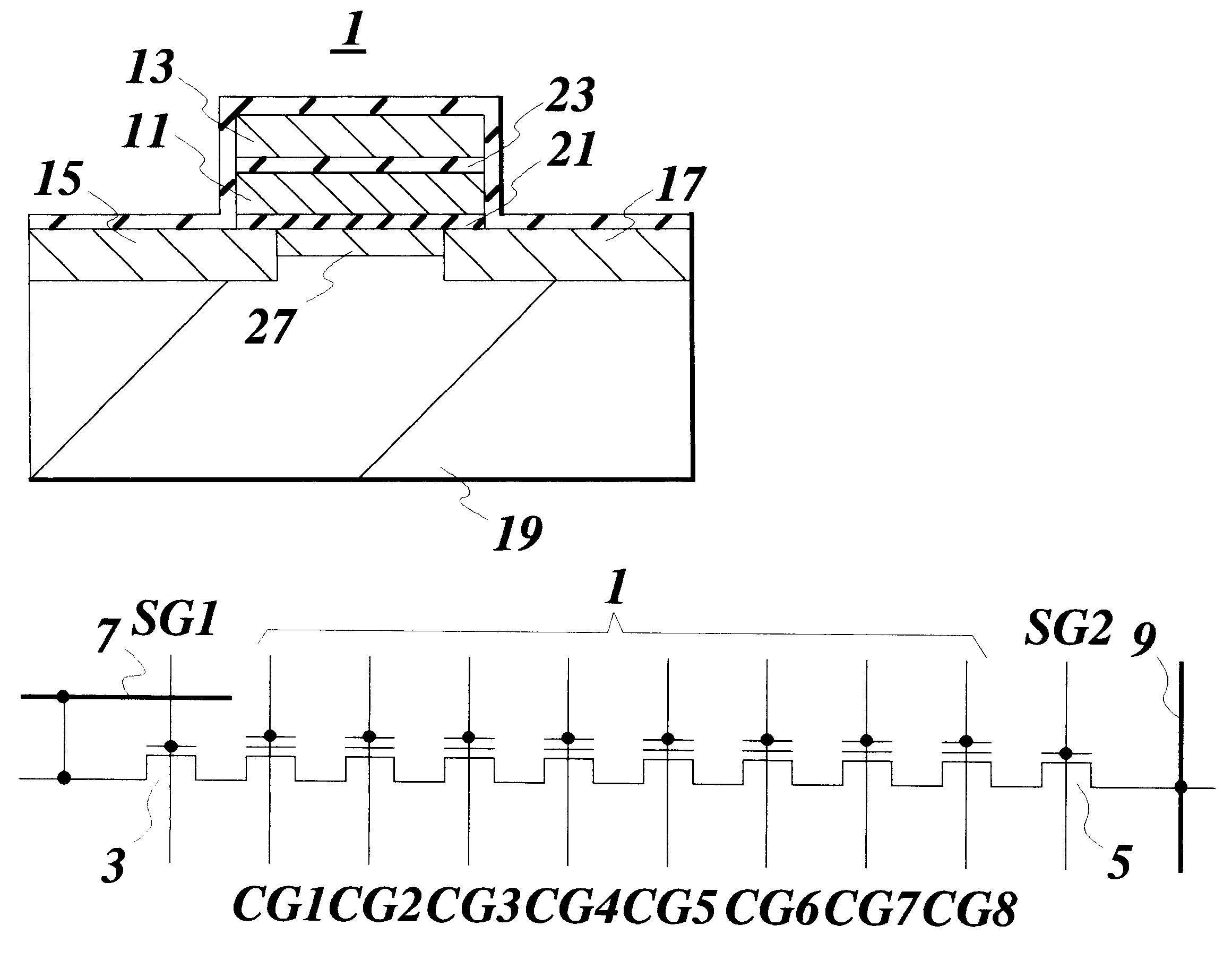
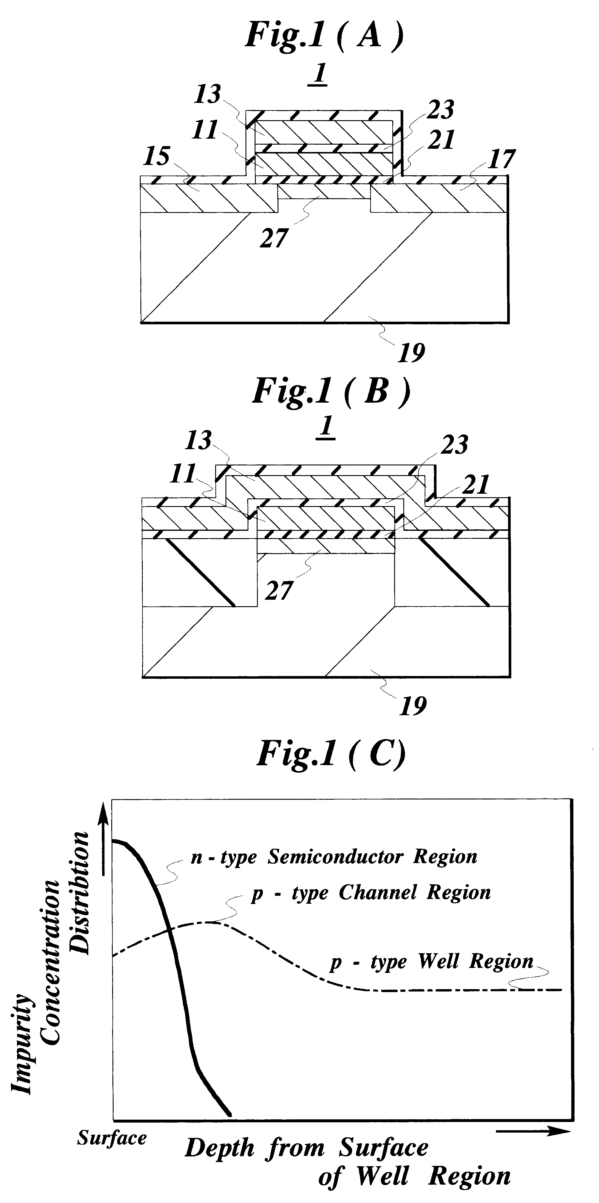
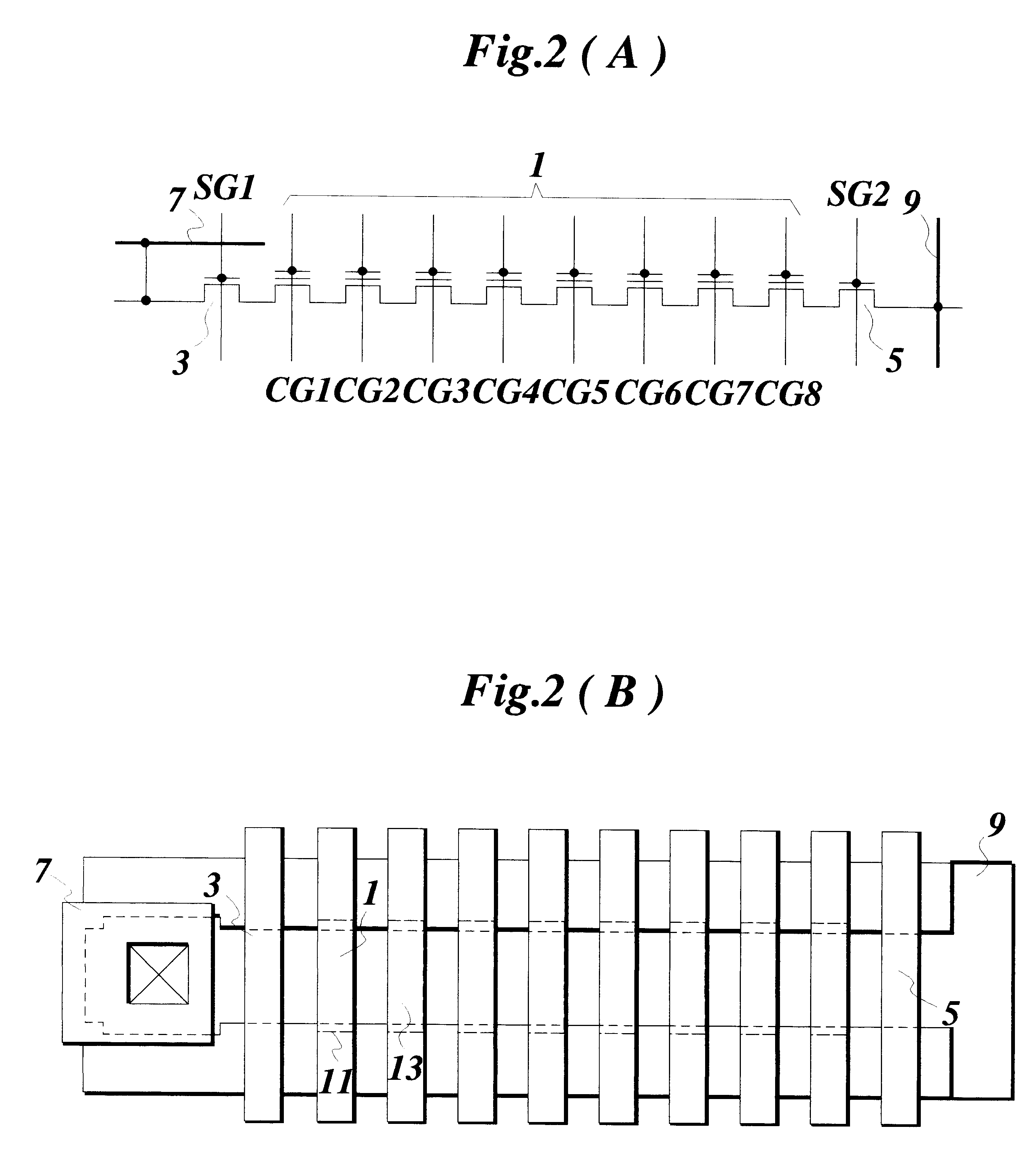
FIG. 2(A) shows an equivalent circuit of a NAND-type EEPROM according to an embodiment of the present invention, and FIG. 2(B) is a plan view showing the EEPROM. The EEPROM has memory cells 1 each having an insulated-gate FET having an information storage part for storing one bit of information. Although the embodiment arranges the memory cells 1 of eight bits in series, the number of memory cells or bits is optional. Among the eight memory cells 1, the adjacent insulated-gate FETs share a source or drain region, and the eight memory cells 1 are electrically connected in series. In the embodiment, the insulated-gate FET is of an n-channel type to r...


PUM


Abstract

A nonvolatile semiconductor memory has memory cells (1) each having an insulated-gate FET that has an information storage part. A semiconductor region (27) is formed at the surface of a channel region of each memory cell. The semiconductor region has the same conductivity type as a channel conductivity type and functions to decrease the strength of an electric field at the surface of the channel region. If the insulated-gate FET is of an n-channel type, the semiconductor region is of an n-type. The semiconductor region suppresses threshold voltage variations among the insulated-gate FETs of the memory cells and prevents soft-writing in the memory cells.

Description

1. Field of the InventionThe present invention relates to an erasable and programmable nonvolatile semiconductor memory, semiconductor integrated circuit device having the semiconductor memory and method of manufacturing the semiconductor memory. In particular, the present invention relates to an EEPROM (electrically erasable and programmable read-only memory) capable of suppressing threshold-voltage variations among memory cells and preventing soft-writing (erroneous writing) in memory cells, semiconductor integrated circuit device having the EEPROM and a method of manufacturing such an EEPROM.2. Description of the Prior ArtSemiconductor memories are roughly classified into RAMs (random-access memories) and ROMs (read-only memories). The RAMs allow to rewrite information stored therein at any time. The ROMs allow to write information into them during manufacturing or after manufacturing, and the information once written therein is completely unable to rewrite or is difficult to rew...

Claims


Application Information

Patent Timeline
Patent Type & Authority Patents(United States)
IPC IPC(8): G11C16/04G11C11/56H01L27/115H01L29/66H01L21/70H01L21/8247H01L29/788H01L29/792
CPCG11C11/5621G11C11/5628G11C11/5635G11C16/0483H01L27/115H01L27/11521H01L29/7883H10B69/00H10B41/30
Inventor SHIGYO, NAOYUKI
Owner KK TOSHIBA
Why Eureka
Try Eureka