Organic films and a process for producing fine pattern using the same

a technology of organic films and fine patterns, applied in the direction of liquid surface applicators, coatings, nanotechnology, etc., can solve the problems of insufficient acid and alkali resistance and durability of monomolecular films, inability to form limited combinations of functional groups and substrates, and weak bonding between substrates and monomolecular films

Inactive Publication Date: 2001-05-01
NEW ENERGY & IND TECH DEV ORG 45
View PDF6 Cites 22 Cited by
  • Summary
  • Abstract
  • Description
  • Claims
  • Application Information

AI Technical Summary

Problems solved by technology

Due to the nature of the LB film, however, the interaction between the substrate and the monomolecular film is very weak and the acid and alkali resistance and durability of the film are insufficient for the construction of complex devices.
The SA film does not have the disadvantages of the LB film, but due to the use of chemical adsorption between the functional groups and the substra

Method used


Image

  • Organic films and a process for producing fine pattern using the same
  • Organic films and a process for producing fine pattern using the same
  • Organic films and a process for producing fine pattern using the same

Examples


embodiment 1

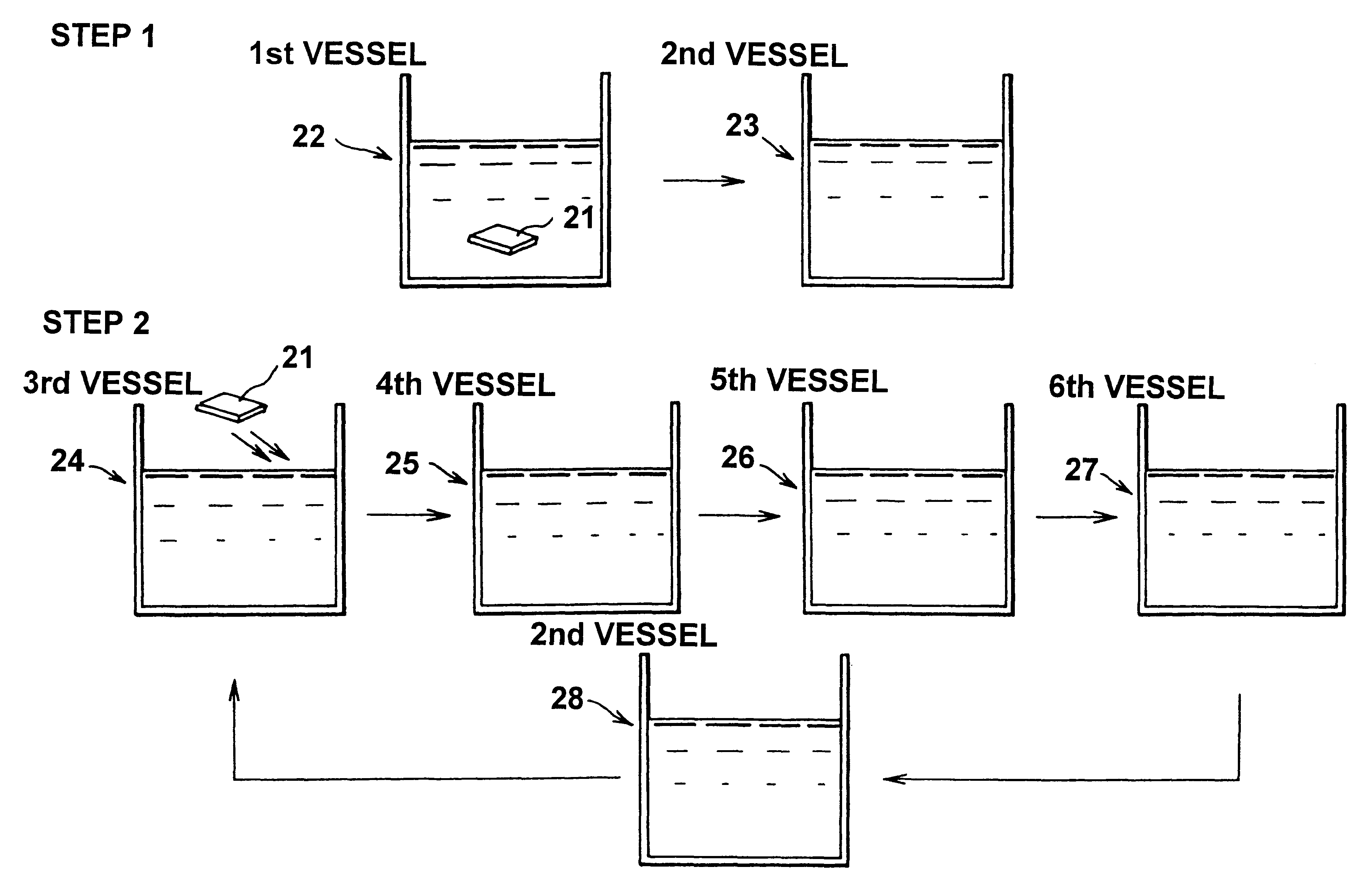
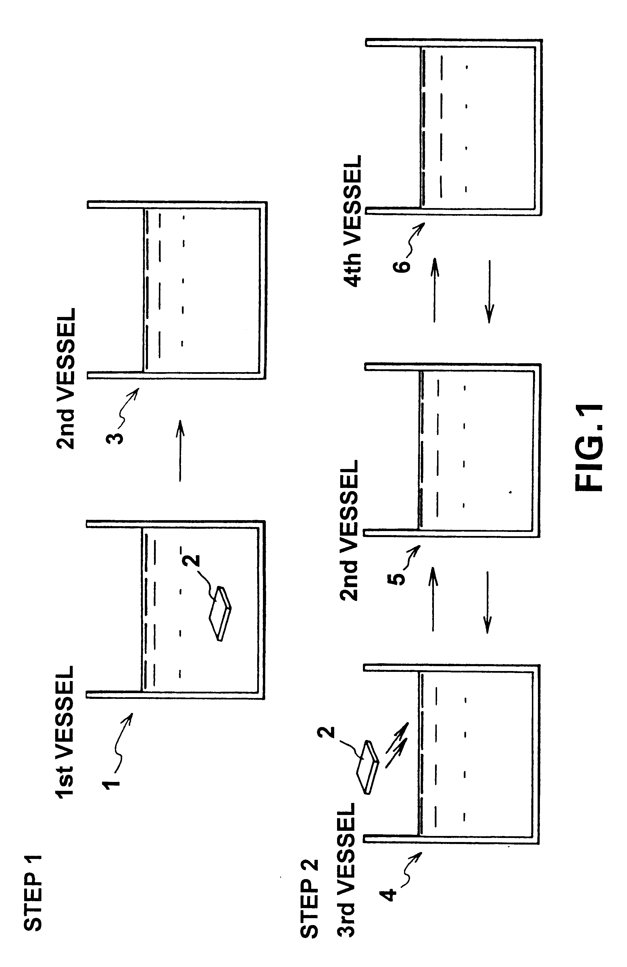
FIG. 1 illustrates one embodiment that creates an organic multilayer film according to this invention. In this figure, a first vessel 1 contains an ethanol solvent and a 1-mM 1,18-octadecylbisphosphonic acid [H.sub.2 O.sub.3 P(CH.sub.2).sub.18 PO.sub.3 H.sub.2 ](here after referred to as "ODBP) solution. To create an organic film, the surface of a GaAs substrate 2 is cleaned using a mixed solution of H.sub.2 O.sub.2 and H.sub.2 SO.sub.4, and the substrate is subsequently washed in pure water, dried, and then immersed in the solution contained in the first vessel. During the chemical adsorption of ODBP, the solution may be maintained at room temperature or may be heated. The solvent may be an organic solvent other than the ethanol solution, or may be pure water, but the organic solvent is preferable. The GaAs substrate 2 remains immersed in the solution contained in the first vessel 1 for several (as an example, four) hours, and is them removed therefrom and washed in pure ethanol co...

embodiment 2

FIG. 3 illustrates another embodiment that creates an organic multilayer film according to this invention. In this figure, a first vessel 8 contains an ethanol solvent and a 1-mM ODBP solution. To create an organic film, the surface of a GaSb substrate 7 is cleaned with a mixed solution of H.sub.2 O.sub.2 and H.sub.2 SO.sub.4, and the substrate is then washed in pure water, dried, and immersed in the solution contained in first vessel 8. The ODBP may be used in powder or liquid form. During the chemical adsorption of ODBP, the solution may be maintained at room temperature or may be heated. The solvent may be an organic solvent other than the ethanol solution, or may be pure water, but an organic solvent is preferable. The GaSb substrate 7 remains immersed in the solution contained in the first vessel 8 for several (five, as an example) hours, and is then removed therefrom and washed in pure ethanol contained in a second vessel 9 to remove the excess molecules deposited on the surfa...

embodiment 3

FIG. 4 illustrates yet another embodiment that creates an organic multilayer film according to this invention. In this figure, a first vessel 14 contains a 19-acetoxynonadecylphosphonic acid [H.sub.3 CO.sub.2 C(CH.sub.2).sub.17 PO.sub.3 H.sub.2 ] solution. To create an organic film, an InSb substrate 13 is cleaved in this solution, contained in first vessel 14. The surface of the substrate 13 can be processed as in Embodiment 1. 19-acetoxynonadecylphosphonic acid may be used in powder or liquid form. During the chemical adsorption of 19-acetoxynonadecylphosphonic acid, the solution may be maintained at room temperature or may be heated. The solvent may be an organic solvent other than the ethanol solution, or may be pure water, but an organic solvent is preferable. The InSb substrate 13 remains immersed in the solution contained in the first vessel 14 for several hours, and is then removed therefrom and washed in pure ethanol in a second vessel 15 to remove the excess 19-acetoxynona...


PUM


Abstract

This invention provides a process for accumulating different organic molecular films on oxidized III-V-group compound semiconductor substrates in order to produce a stable, high-quality organic monomolecular film that is three-dimensionally regularly arranged, as well as a process for producing a fine pattern of such organic films. This organic film is formed by immersing a III-V group compound semiconductor substrates in a vessel containing a solution containing phosphonic acid dissolved into a solvent in order to form a self-assembled film, and placing the substrate into a different solution to adsorb metal ions to the surface of the film, or immersing the substrate in a bromide or an acid or alkali solution to denature functional groups, then immersing it in a solution containing organic molecules that are selectively chemically adsorbed to the modified functional groups. These steps are repeated to form a stable, high-quality multilayer film that is three-dimensionally regularly arranged, while controlling film thickness with an accuracy on the scale of thickness of a molecular layer.In addition, the present invention realizes the formation of a fine composite three-dimensional organic self-assembled film of the order of nanometer, characterized in that the process comprises using a cleavage method or a very-high-vacuum vessel to form on a substrate with different types of III-V-group semiconductor materials mixed thereon by means of the heteroepitaxial process such as the MBE or MOCVD process, a self-assembled film of the molecules having thiol groups in a non-oxidized area and then forming on an oxidized surface a self-assembled film of molecules having phosphoric acid group, trichlorosilyl groups or alkoxylyl groups.

Description

The present invention relates to a process for manufacturing a monomolecular film and an organic built-up film that are two-dimensionally regularly arranged on both an oxidized and a bare III-V-group compound semiconductor substrate, and to a method for producing a fine pattern using the organic films.DESCRIPTION OF THE PRIOR ARTLangmuir Blodgett films (hereafter referred to as "LB films") and self-assembled monolayers (hereafter referred to as "SA films") are the well known types of organic monomolecular films or organic built-up films (Abraham Ulman, "An Introduction to Ultrathin Organic Films From Langmuir-Blodgett to Self-Assembly," Academic Press 1991). Of the two, the LB film is formed by developing amphiphilic molecules having both hydrophilic and hydrophobic atomic groups, on the water surface as a monomolecular film (an "L film"), transferring the film to a solid substrate, and accumulating a number of films thereon. The LB film is named after Langmuir and Blodgett, who dev...

Claims


Application Information

Patent Timeline
IPC IPC(8): B05D1/18H01L21/02H01L21/312
CPCB05D1/185B82Y30/00B82Y40/00H01L21/3128H01L21/02285
Inventor OHNO, HIROTAKAFUJIOKA, KAZUSHIYAMANAKA, MIKIHIROMITARAI, SATOKOTOKUMOTO, HIROSHI
Owner NEW ENERGY & IND TECH DEV ORG 45
Why Eureka
Try Eureka