Selective reduction of sidewall slope on isolation edge

a transistor and isolation edge technology, applied in semiconductor devices, instruments, photomechanical treatment, etc., can solve the problems of inability to meet the requirements of many manufacturing methods, non-flat wafers, and non-uniform bakes, so as to reduce device off-current and reduce sidewall slope

Inactive Publication Date: 2001-05-08
IBM CORP
View PDF50 Cites 27 Cited by
  • Summary
  • Abstract
  • Description
  • Claims
  • Application Information

AI Technical Summary

Problems solved by technology

Pattern control in photolithographic processes, however, is negatively impacted by numerous effects ranging from resist thickness variations, bake non-uniformities, non-flat wafers, etc.
The resist profiles shown are strongly re-entrant on both sides of the pattern which is not acceptable for many manufacturing methods.
The presence of the semiconductor corner in the active device region (active area) of a surface-channel trench bounded MOSFET, for example, results in a parasitic leakage current between source and drain diffusions.
It has been found that the leakage current along the corner of the MOSFET results from a local lowering of the threshold voltage, due to the geometry of the device.
In addition to increased leakage current, the enhanced corner electric field results in degraded device reliability.
It has been discovered that the device off-current is sensitive to the sidewall angle of the active area.
It is a disadvantage of known structures employing trench isolation for the purpose of isolation of adjacent active devices (e.g. transistors), that the device-off current (in particular for array transistors) is relatively high.

Method used


Image

  • Selective reduction of sidewall slope on isolation edge
  • Selective reduction of sidewall slope on isolation edge
  • Selective reduction of sidewall slope on isolation edge

Examples


Embodiment Construction

)

In describing the preferred embodiments of the present invention, reference will be made herein to FIGS. 1-9 of the drawings in which like numerals refer to like features of the invention. Features of the invention are not necessarily shown to scale in the drawings.

Polysilicon (also referred to as polycrystalline silicon) can be formed using chemical vapor deposition (CVD), or low pressure chemical vapor deposition (LPCVD), as well as other known processes. Polysilicon is a solid composed of a myriad of small single crystal regions.

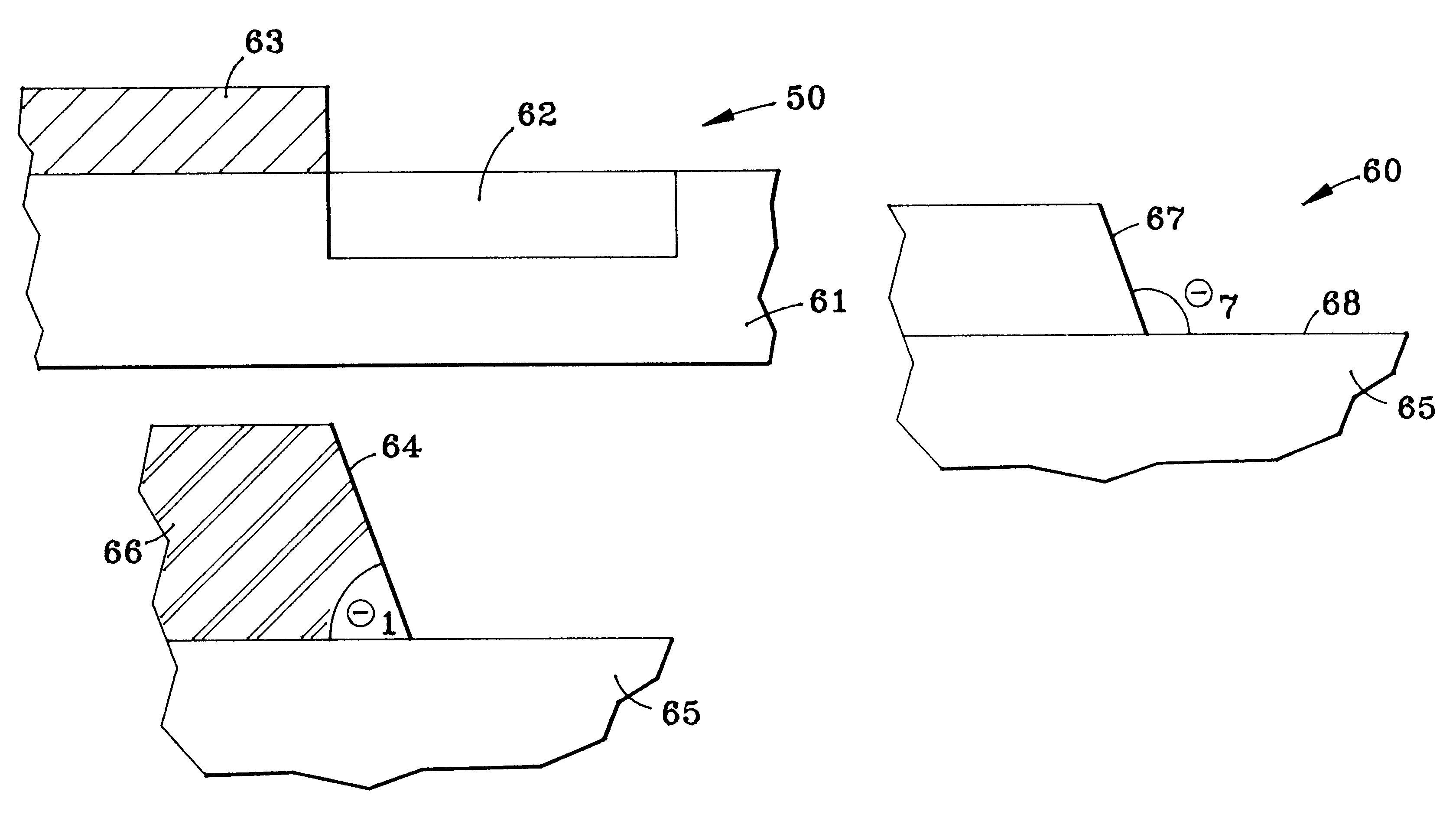
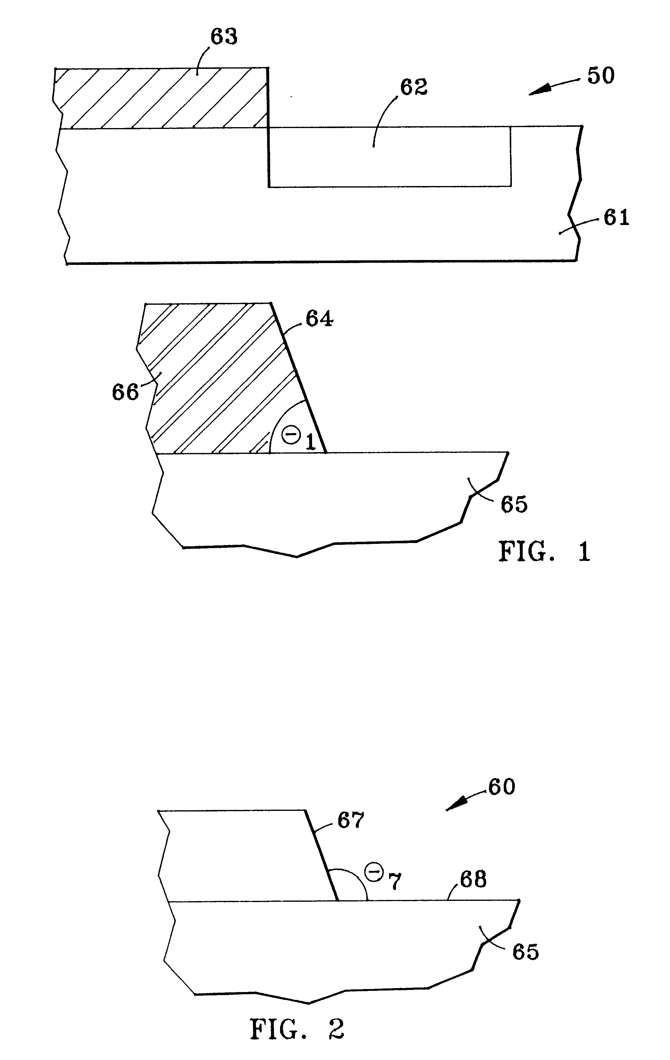
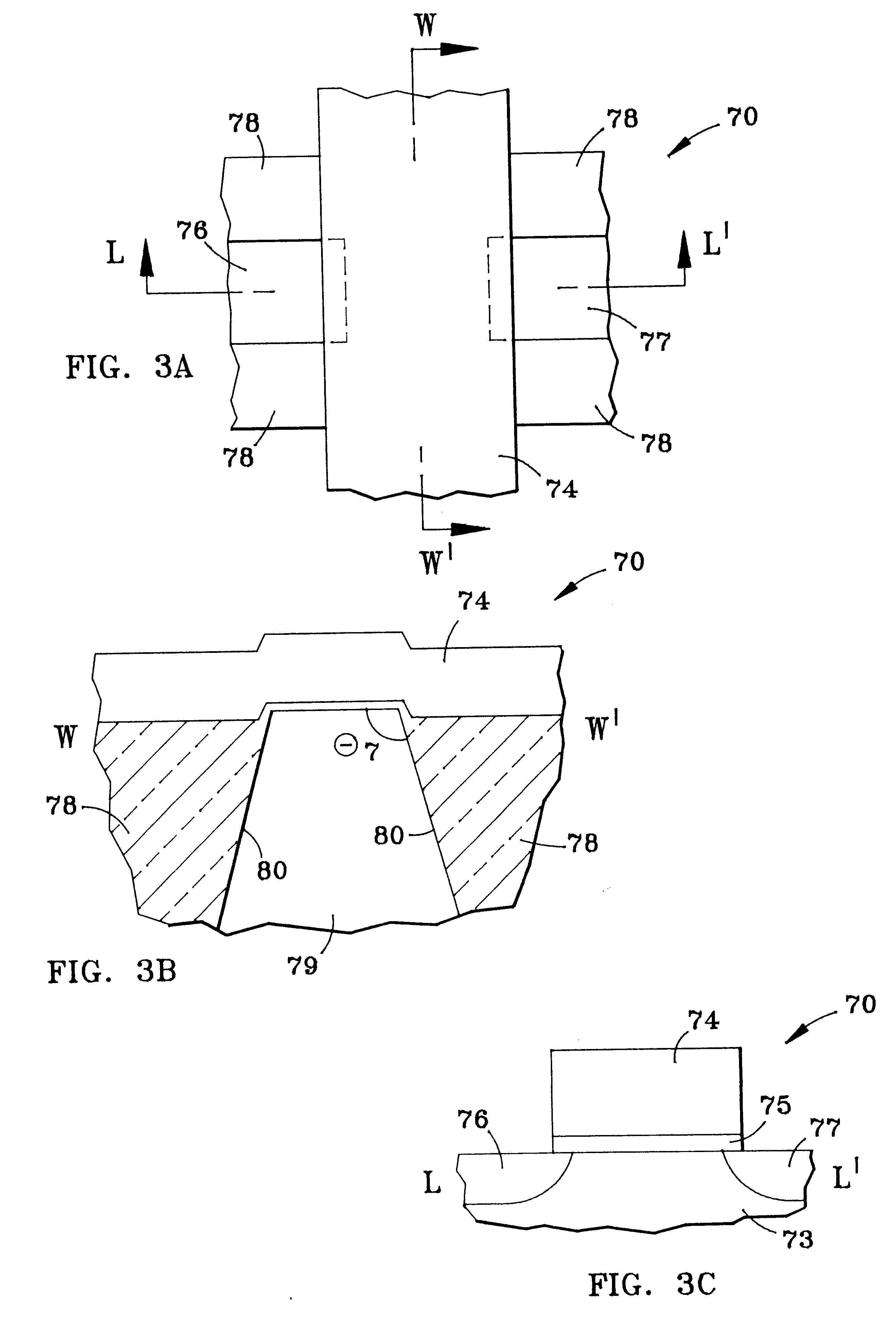
FIGS. 1 and 2 together with FIGS. 4-8 are used to describe how the inventive structure shown in FIGS. 3A-3C can be made.

In FIG. 1, a cross section of special mask 50 is shown. This mask has a substrate 61 (e.g. glass), a chrome line 63 and a window 62 which was etched away. By etching away a certain thickness of the substrate 61 adjacent to the chrome 63, the phase shift of the light penetrating through the mask 50 can be controlled. Details of such mask...


PUM


Abstract

Disclosed is a semiconductor structure which comprises a transistor having a source implantation and a drain implantation formed in a semiconductor substrate. The transistor further comprises a gate electrode, a gate oxide, and an active area. The source implantation and drain implantation are situated on opposite sides of said active area, and said gate oxide and gate electrode are situated on top of said active region. The transistor further comprises two trench isolations adjacent to said active area, wherein said trench isolations are situated on opposite sides of said active area such that a sidewall of each trench serves as interface to said active area, at least one of said sidewalls of said trench isolations which serves as interface to said active area being sloped having a slope between 90° and 150°,said trench isolations and source implantation and drain implantation enclosing said active area on four sides.

Description

1. Cross-reference to Related Patent ApplicationsThis patent application is related to U.S. patent application Ser. No. 08 / 820,401 entitled "Asymmetrical Field Effect Transistor", and U.S. Pat. No. 5,948,571 entitled "Asymmetrical Resist Sidewall", both filed on the same day as the instant application and both being presently assigned to the assignee of the instant application and the disclosure of which is incorporated herein by reference. This application is further related to U.S. patent application Ser. No. 09 / 175,856 filed Oct. 20, 1998 entitled "Asymmetrical Resist Sidewall," the same being a Divisional application of said U.S. Pat. No. 5,948,571.2. Field of the InventionThis invention relates to trench bounded transistors, and in particular trench bounded metal oxide semiconductor (MOS), or complentary metal oxide semiconductor (CMOS), or silicon on insulator (SOI), field effect transistors.3. Description of Related ArtIn electronic component manufacture and in particular int...

Claims


Application Information

Patent Timeline
Patent Type & Authority Patents(United States)
IPC IPC(8): H01L21/70H01L21/762H01L21/76H01L21/8238H01L27/092H01L29/78H01L29/786
CPCH01L21/76232Y10S438/947
Inventor WHEELER, DONALD C.HSU, LOUIS L.MANDELMAN, JACK A.MIH, REBECCA D.
Owner IBM CORP
Why Eureka
Try Eureka