Semiconductor device and method of fabricating the same

a technology of semiconductor devices and semiconductors, applied in semiconductor devices, semiconductor/solid-state device details, electrical apparatus, etc., can solve the problems of increasing the propagation delay of signals, affecting the processing speed of signals, and difficult to be processed or patterned by ordinary dry etching processes at low temperatures

Inactive Publication Date: 2001-06-12
NEC CORP
View PDF6 Cites 337 Cited by
  • Summary
  • Abstract
  • Description
  • Claims
  • Application Information

AI Technical Summary

Problems solved by technology

Conventionally, the operation speed of transistors has bean gradually raised according to their consecutive dimensional reduction However, in LSIs fabricated under the design rule of 0.18 .mu.m or less, it has been found that the signal processing speed is affected more by the propagation delay of signals in wiring lines than by the operation speed of transistors.
Since Cu is lower in vapor pressure than that of halides, it is difficult to be processed or patterned by ordinary dry etching processes at low temperatures.
This increases largely the propagation delay of signals.
However, these methods have other problems explained below.
In other words, low relative dielectric constants of there layers are difficult to be realized as desired.
Consequently, they cause a problem that the propagation delay of signals cannot be suppressed effectively.
Moreover, the organic dielectric layers necessitate complicated process steps of removing resist films used for patterning the same organic dielectric layers.
This means that they cause another problem that the fabrication cost of LSIs becomes higher.

Method used


Image

  • Semiconductor device and method of fabricating the same
  • Semiconductor device and method of fabricating the same
  • Semiconductor device and method of fabricating the same

Examples


first embodiment

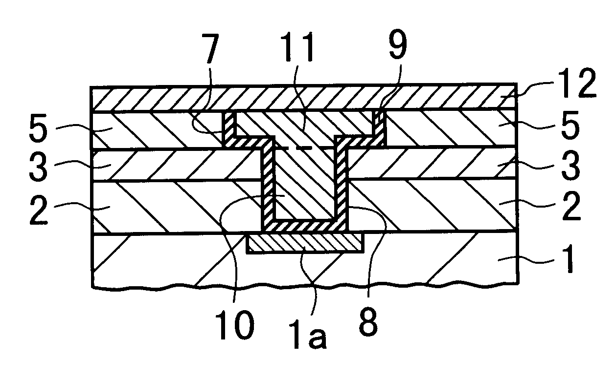
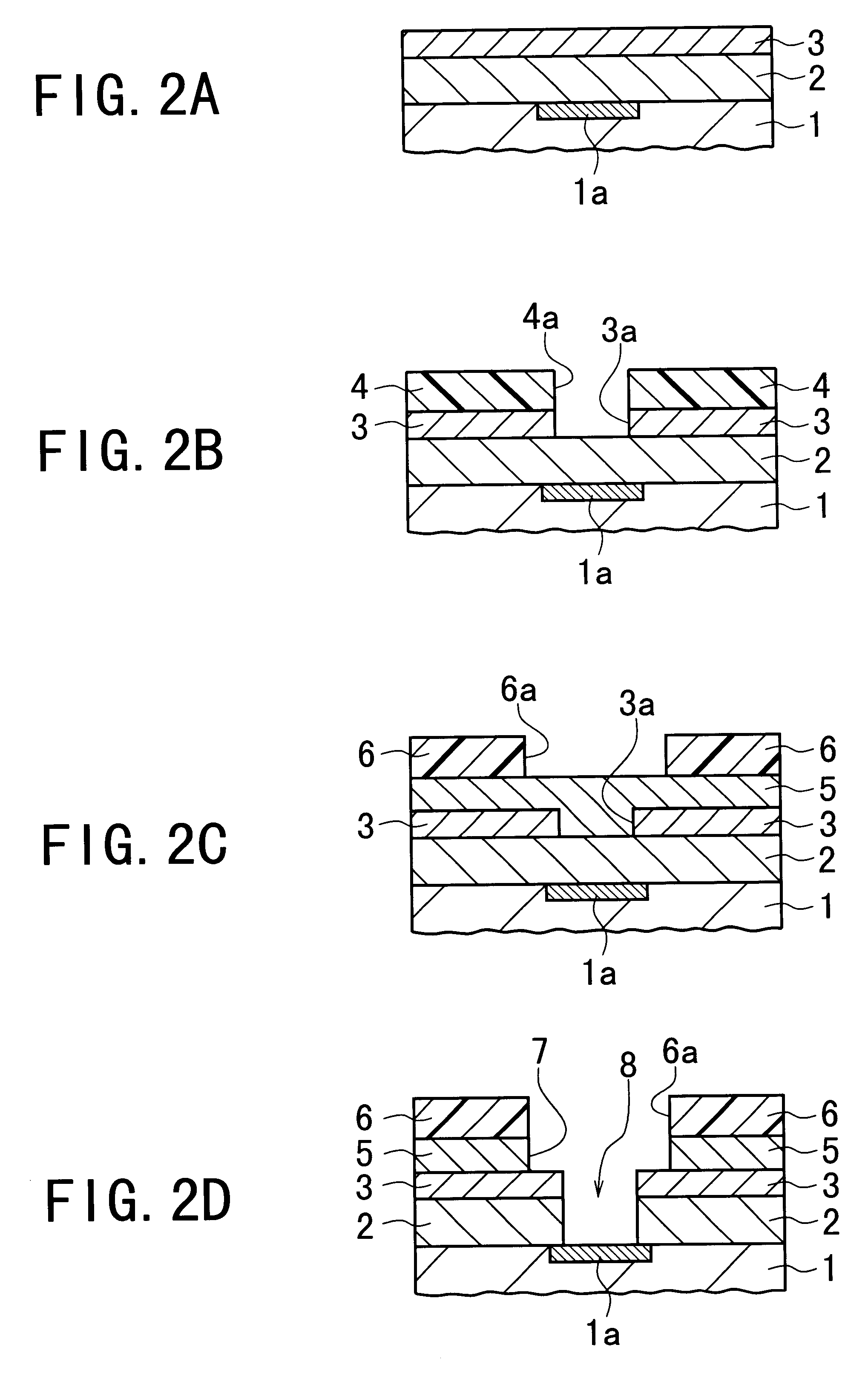
FIGS. 2A to 2G show a method of fabricating a semiconductor device which uses the dual damascene process.

First, as shown in FIG. 2A, a single-crystal silicon substrate 1 having specific electronic elements such as transistors and am least one wiring layer is prepared. Only a diffusion region 1a of one of the elements is illustrated in FIG. 2A for the sake of simplification.

Then, a first interlayer dielectric layer 2 with a thickness of 100 to 800 nm is formed on the surface of the substrate 1 by a plasma-enhanced CVD process. The layer 2 is made of plasma-deposited SiO.sub.2, fluorinated plasma-deposited SiO.sub.2 (i.e., SiOF), or HSQ.

Next, a second interlayer dielectric layer 3 with a thickness of 50 to 400 nm is formed on the first interlayer dielectric layer 2. The layer 3 is made of SiO.sub.2 containing carbon of 5 to 30 weight % (wt. % ). If the carbon content is greater than 30 wt. %, the layer 3 will have similar property to that of the organic dielectric layers, resulting i...

second embodiment

FIGS. 3A to 3E show a method of fabricating a semiconductor device according to a second embodiment. This method also uses the dual damascene process.

First, as shown in FIG. 3A, a single-crystal silicon substrate 1 having specific electronic elements such as transistors and at least one wiring layer is prepared. Only one diffusion region 1a is illustrated in FIG. 3A as one of the elements for the sake of simplification. Then, a first interlayer dielectric layer 2 with a thickness of 100 to 800 nm is formed on the surface of the substrate 1 by a plasma-enhanced CVD process. The layer 2 is made of plasma-deposited SiO.sub.2, fluorinated plasma-deposited SiO.sub.2 (i.e., SiOF), or HSQ.

Next, a second interlayer dielectric layer 3 with a thickness of 50 to 400 nm is formed on the first interlayer dielectric layer 2. The layer 3 is made of SiO.sub.2 containing carbon of 5 to 30 wt. %. The layer 3 is formed by the same method as shown in the first embodiment.

The above process steps are the...


PUM


Abstract

A semiconductor device equipped with the dual damascene structure that is provided, which suppresses the propagation delay of signals effectively without using any complicated processes. The device is comprised of (i) a semiconductor substrate having a lower wiring layer and electronic elements; (ii) a first interlayer dielectric layer formed on the substrate; (iii) a second interlayer dielectric layer formed on the first interlayer dielectric layer, the second interlayer dielectric layer being made of carbon-containing SiO2; (iv) a third interlayer dielectric layer formed on the second interlayer dielectric layer; (v) a fourth interlayer dielectric layer formed on the third interlayer dielectric layer, the fourth interlayer dielectric layer being made of carbon-containing SiO2; (vi) the first and second interlayer dielectric layers having a via hole penetrating therethrough; (vii) the third interlayer dielectric layer having a recess overlapping with the via hole, the recess being formed to communicate with the via hole; (viii) a metal plug formed in the via hole to be contacted with the lower wiring layer or the electronic elements in the substrate; (ix) a metal wiring layer formed in the recess; and (x) a fourth interlayer dielectric layer formed on the third interlayer dielectric layer to cover the metal wiring layer.

Description

1. Field of the InventionThe present invention relates to a semiconductor device and a method of fabricating the same and more particularly, to a semiconductor device with the dual damascene structure in which the wire-to-wire capacitance is reduced and the propagation delay of signals is suppressed, and a method of fabricating the device without using any complicated process steps.2. Description of the Prior ArtIn recent years, there has been the increasing need to raise the speed of signal processing in semiconductor devices, especially in Large-Scale Integrated circuits (LSIs). The signal processing speed in LSIs is mainly dependent upon the operation speed of individual transistors and the delay of signals propagating through wiring lines.Conventionally, the operation speed of transistors has bean gradually raised according to their consecutive dimensional reduction However, in LSIs fabricated under the design rule of 0.18 .mu.m or less, it has been found that the signal process...

Claims


Application Information

Patent Timeline
Patent Type & Authority Patents(United States)
IPC IPC(8): H01L21/02H01L21/70H01L21/768H01L21/316H01L21/3205H01L21/28H01L23/52H01L23/522
CPCH01L21/02126H01L21/02131H01L21/02134H01L21/02164H01L21/022H01L21/02274H01L21/02282H01L21/31633H01L21/76801H01L21/76807H01L21/7681H01L21/76829H01L21/76834H01L2221/1036H01L21/28
Inventor YOKOYAMA, TAKASHI
Owner NEC CORP
Why Eureka
Try Eureka