Method and apparatus for electronically controlled scanning of micro-area devices

a micro-area device and electronic control technology, applied in the direction of instruments, optical elements, discharge tubes/lamp details, etc., can solve the problems of limiting the number of capillaries or microchannels on the chip, limiting the number of microchannels that can be effectively utilized on the microchip, and limiting the image processing time for real-time analysis

Inactive Publication Date: 2001-06-12
PITTSBURGH UNIV OF
View PDF25 Cites 29 Cited by
  • Summary
  • Abstract
  • Description
  • Claims
  • Application Information

AI Technical Summary

Problems solved by technology

However, the number of the capillaries or microchannels on a chip is limited by the resolution and sensitivity of the CCD camera.
Because the CCD acquires the image through a large amount of stored data, the image processing time for real-time analysis is another obstacle, limiting the number of microchannels that can be effectively utilized on the microchip.
Another obvious drawback is the full-field illumination.
First, a long illumination time will increase photodynamic damage and dye bleaching.
This second disadvantage will eventually restrict the channel number on a given chip.
There is no limitation to the number of the capillaries or multi-channels, but as a result of the mechanical movement with this method, it is difficult to realize

Method used


Image

  • Method and apparatus for electronically controlled scanning of micro-area devices
  • Method and apparatus for electronically controlled scanning of micro-area devices
  • Method and apparatus for electronically controlled scanning of micro-area devices

Examples


Embodiment Construction

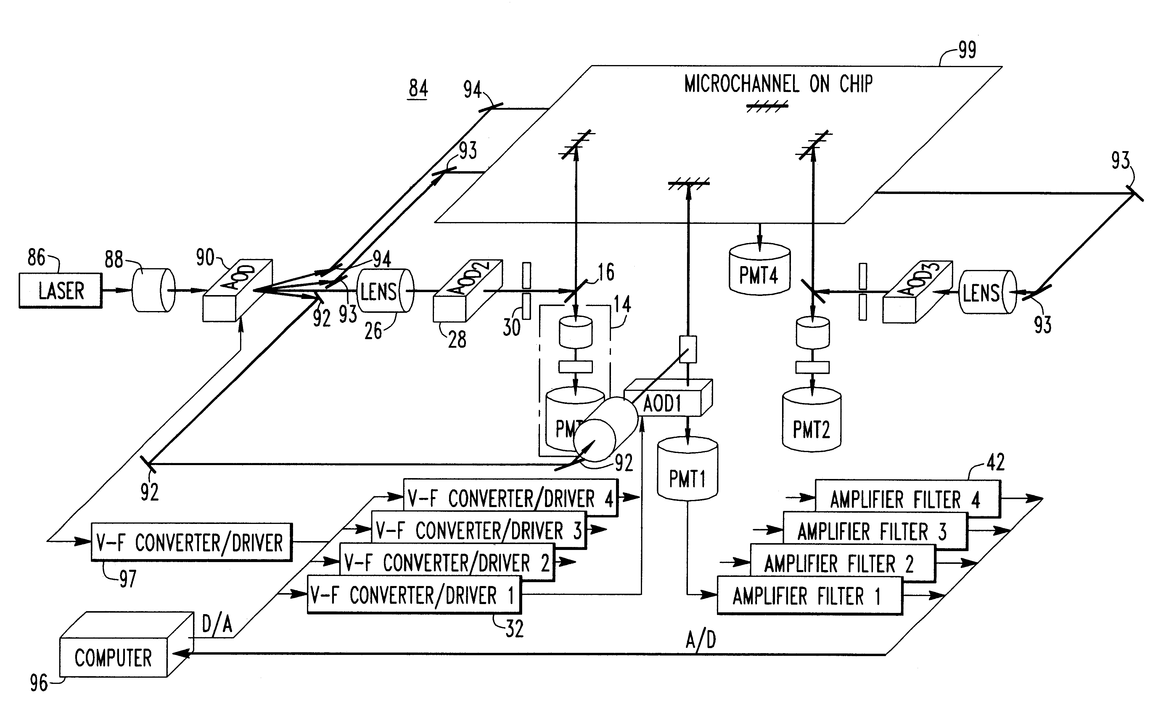
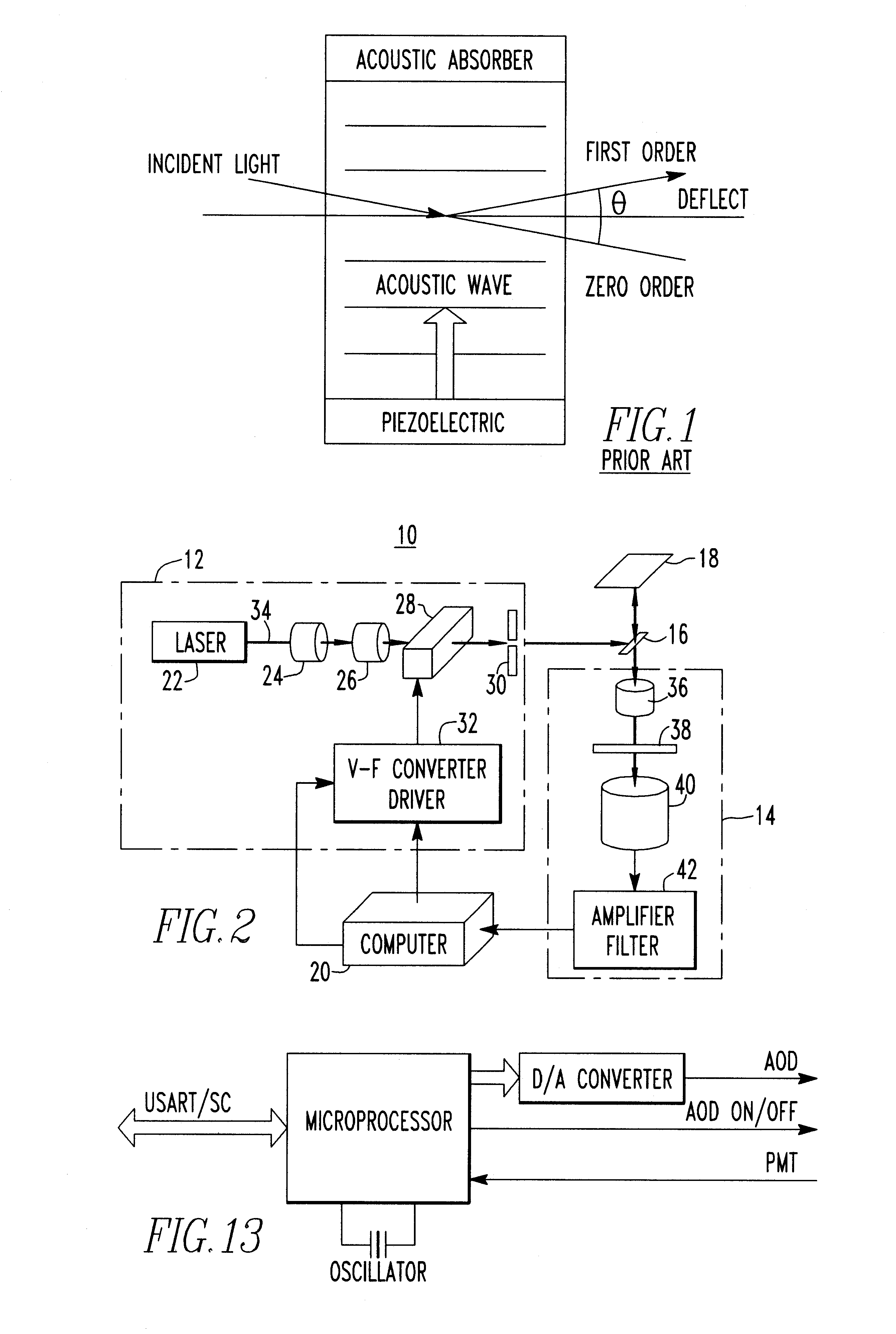
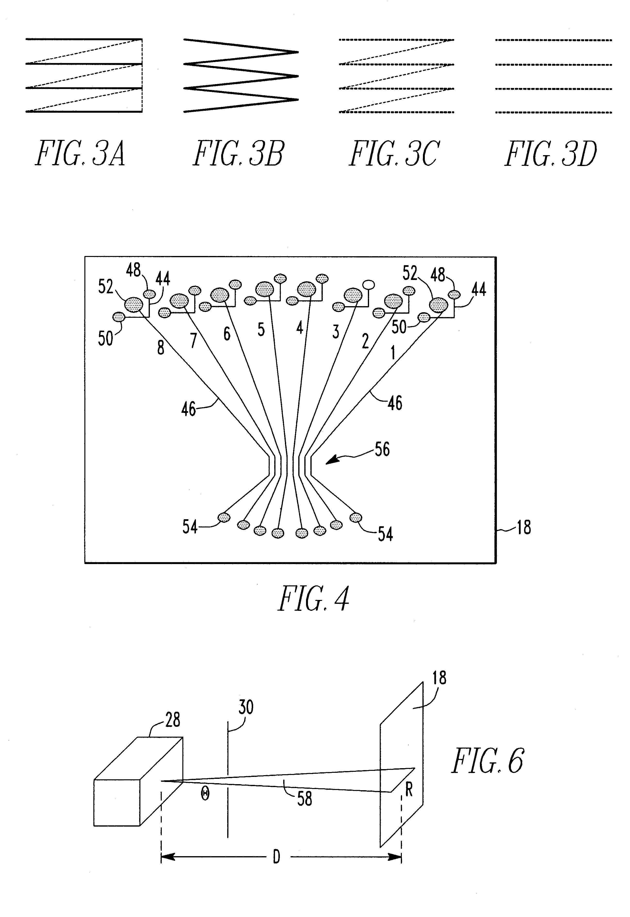
FIG. 2 illustrates a system 10 constructed according to the teachings of the present invention. The system 10 is comprised of three major components; an excitation source 12, a detector 14, and a device or means 16 for optically coupling the excitation source 12 and the detector 14 to a target 18. In the embodiment of the system 10 shown in FIG. 2, a dichroic beam splitter is used as the device 16. In that manner, the target may be excited or illuminated, and fluorescence detected, from the same side of the target. The reader will recognize, however, that other types of devices 16, which are well known in the art, may be utilized such that the target is illuminated from one side of the system 10 and fluorescence is detected from another side of the system 10. The target 18 illustrated in FIG. 2 is an electrophoresis chip 18. However, the reader should recognize that other types of targets may be used, particularly capillaries or other devices having microchannels, micro-arrays or ot...


PUM


Abstract

The present invention provides an excitation source which may be used, for example, in conjunction with the scanning of multi-channel electrophoresis chips or capillary arrays. The excitation source is comprised of a source of light, such as a laser beam. A beam expander, an acousto-optic deflector, and a filter are optically aligned with the source of light. A driver is connected to the acousto-optic deflector for controlling the angle of deflection. A system is disclosed which includes the excitation source, a detector for detecting fluorescence from a target chip, and a beam splitter or other device for optically connecting the excitation source to the chip and for optically connecting the chip to the detector. The excitation source may be based on an acousto-optic deflector, an electrooptic deflector, a piezoelectric deflector, or any other electronically controlled device. Methods of focusing a beam of collimated light and electronically exciting a plurality of micro-areas of a target chip, either serially or in parallel, are also disclosed.

Description

1. Field of the InventionThe present invention is directed generally to non-mechanical scanning techniques and, more specifically, to electronically controlled scanning of micro-area devices such as multi-channel electrophoresis chips, capillary arrays, microtiter plates, matrix hybridization array chips, etc.2. Description of the BackgroundCancer detection and screening utilizing genomic markers has proven very successful for a variety of cancers. These assays typically include amplification of a target sequence followed by separation of the products. Capillary electrophoresis has proven its ability to decrease the separation time requirements over traditional slab gels while maintaining resolution of the DNA fragments for diagnosis. Electrophoretic chips have reduced this separation time requirement even further.Laser-induced fluorescence detection is a fundamental aspect of the burgeoning chip technology being developed for these and other purposes, and has led to the need for th...

Claims


Application Information

Patent Timeline
IPC IPC(8): G02B21/00
CPCG02B21/002
Inventor LANDERS, JAMES P.HUANG, ZHILIHUHMER, ANDREAS
Owner PITTSBURGH UNIV OF
Why Eureka
Try Eureka