Semiconductor package having a heat sink with an exposed surface

a technology of exposed surface and integrated circuit, which is applied in the direction of semiconductor devices, semiconductor/solid-state device details, electrical devices, etc., can solve the problems of chip 102 being easily cracked, delicate and weak in structure, and forming voids in the encapsulan

Inactive Publication Date: 2001-06-12
SILICONWARE PRECISION IND CO LTD
View PDF28 Cites 177 Cited by
  • Summary
  • Abstract
  • Description
  • Claims
  • Application Information

AI Technical Summary

Benefits of technology

It is therefore an objective of the present invention to provide an integrated circuit package with a fully-exposed heat sink, which can...

Problems solved by technology

Third, the chip 102 could be easily cracked during the transfer molding process due to the pressure from the molding resin flow via the circular recessed portions 116a against the chip 102 which is delicate and weak in structure.
This is because that the molding resin flow during the transfer molding process would be blocked by the recessed portions 116a, 116c, thus causing disturbances to the molding resin flow, resulting in the forming of voids in the encapsulant 112.
Hence, the drawback of off-center arrangement in the integrated circuit package of FIG. 5 still exists in t...

Method used


Image

  • Semiconductor package having a heat sink with an exposed surface
  • Semiconductor package having a heat sink with an exposed surface
  • Semiconductor package having a heat sink with an exposed surface

Examples


Embodiment Construction

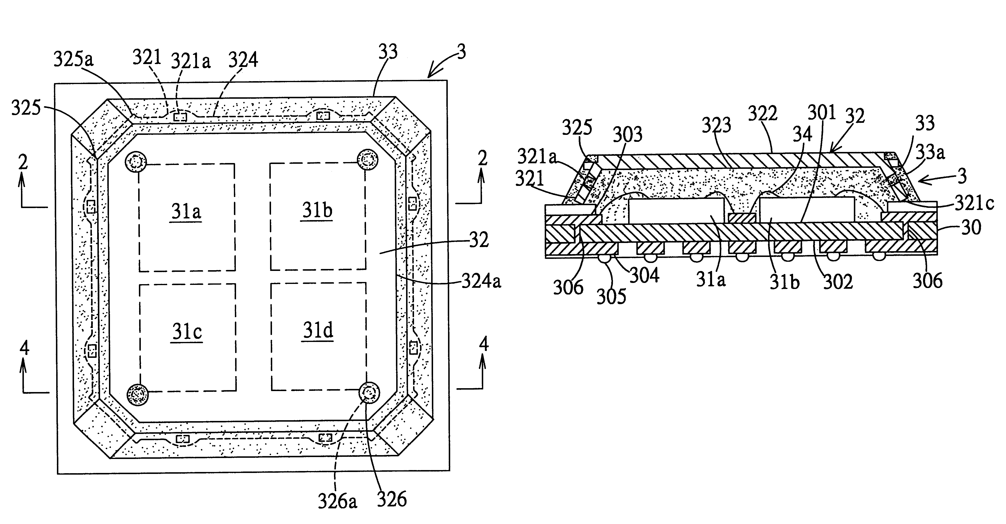
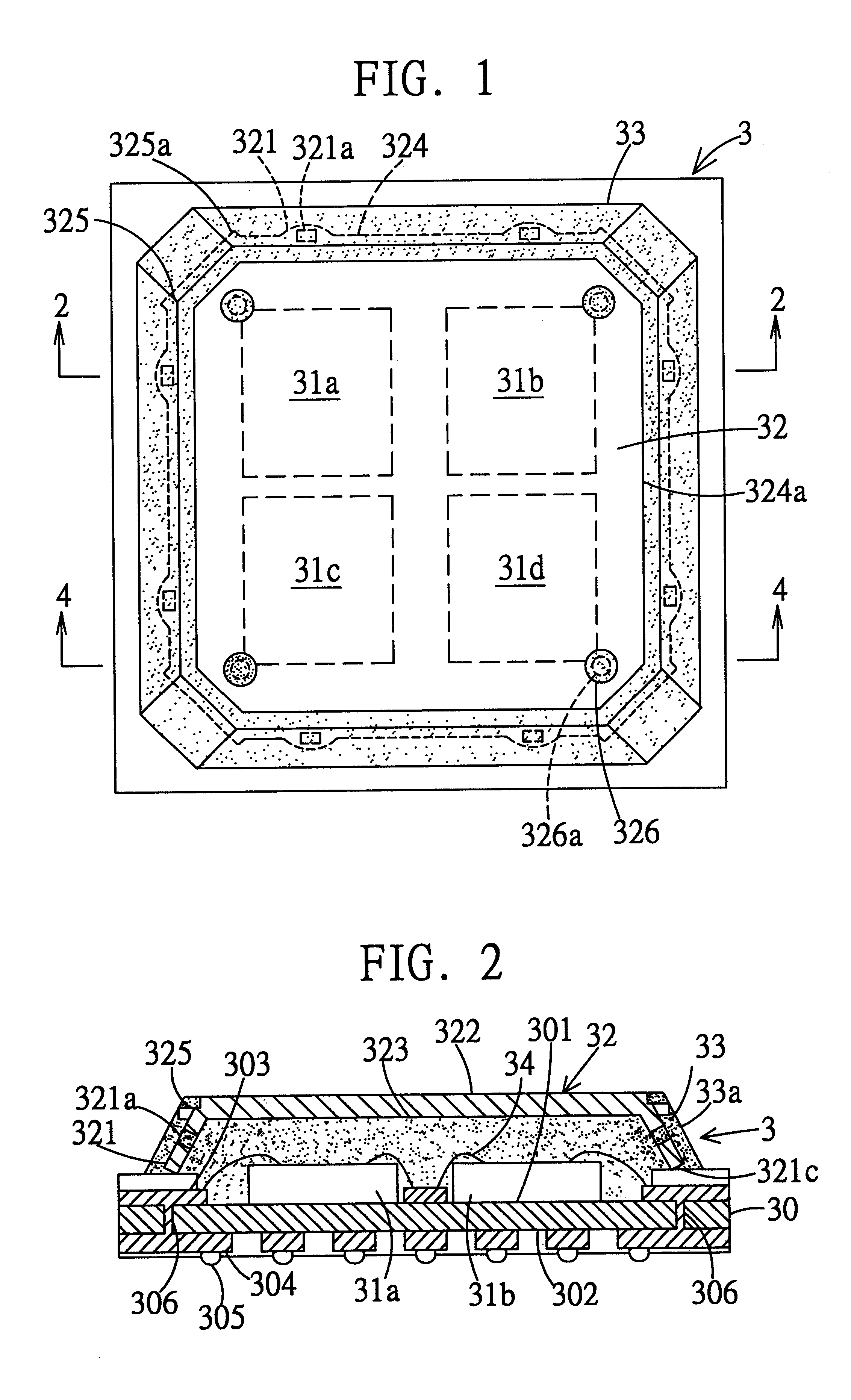
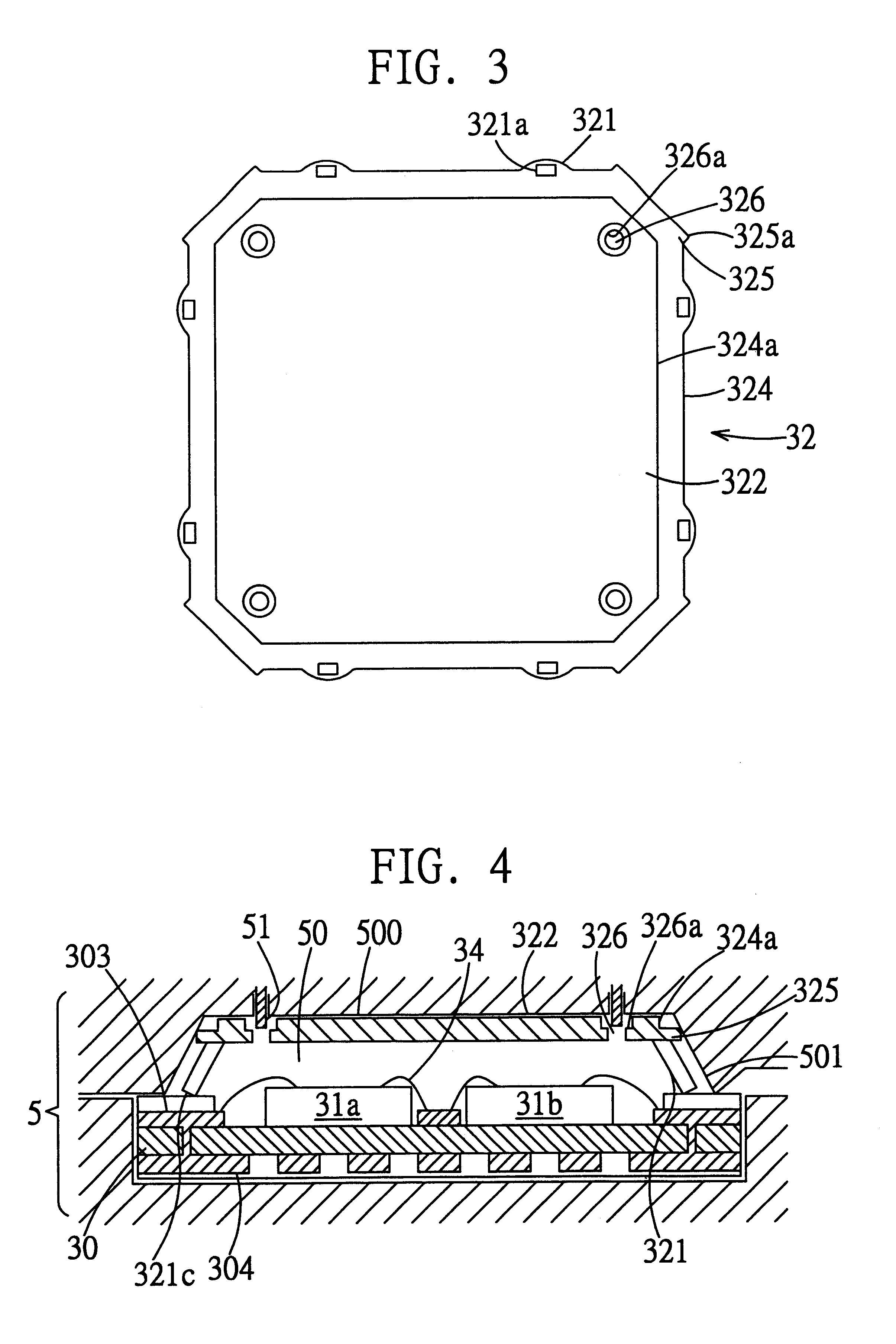
A preferred embodiment of the integrated circuit package of the invention is disclosed in full detail in the following with reference to FIGS. 1-4.

Referring first to FIGS. 1 and 2, the integrated circuit package of the invention includes a substrate 30 (which is used to mount a number of chips 31a, 31b, 31c, and 31d thereon), a heat sink 32 disposed over the substrate 30, and an encapsulant 33 enclosing the chips 31a, 31b, 31c, and 31d and part of the heat sink 32.

The substrate 30 has a first side 301 and a second side 302 opposite to the first side 301. The first side 301 of the substrate 30 is mounted with a first conductive traces 303 which is electrically connected via a plurality of gold wires 34 to the chips 31a, 31b, 31c, and 31d of course, electrical interconnection between the substrate 30 and chips 31a, 31b, 31c, and 31d may instead by made by other conventional methods, such as tape automated bonding (TAB), flip chip bonding, and the like. Further, the second side 302 of ...


PUM


Abstract

An integrated circuit package with a fully-exposed heat sink is provided. The integrated circuit package includes a substrate having a first side being formed with first conductive traces and a second side being formed with second conductive traces. At least one chip is mounted on the substrate and electrically connected to the first conductive traces. A plurality of solder balls are provided at the terminal ends of the second conductive traces to allow external connection of the chip. The fully-exposed heat sink is mounted on the substrate. The heat sink is formed with a plurality of supportive legs arranged in such a manner as to allow a bottom surface of the heat sink to be separated from the chip and a top surface of the heat sink to be tightly attached to a cavity in a mold used to form an encapsulant for enclosing the chip. A plurality of positioning tongues are formed on the heat sink for securing the heat sink in position when performing a molding process for forming the encapsulant. With this integrated circuit package, no jig is required in the assembly of the integrated circuit package. Moreover, since there is no need to use adhesives to adhere the supportive legs onto the substrate, the integrated circuit package would not suffer from delamination as in the case of the prior art. The fully-exposed heat sink allows an increased heat-dissipating efficient as compared to the prior art.

Description

BACKGROUND OF THE INVENTION1. Field of the InventionThis invention relates to integrated circuit package technology, and more particularly, to an integrated circuit package with a heat sink for dissipating heat generated by integrated circuit chip.2. Description of Related ArtAn integrated circuit chip is capable of holding a very great number of circuit components, including resistors, capacitors, and transistors, in a very small semiconductor die. In use, an integrated circuit chip is typically enclosed in a package for easy handling. To allow increased functionality from a single integrated circuit package, a number of integrated circuit chips can be mounted together in one package. This type of integrated circuit package is customarily referred to as a multi-chip-module integrated circuit package.In the manufacture of integrated circuit packages, there are two major topics in design; heat dissipation and pin arrangement. Heat dissipation is typically provided by mounting a heat ...

Claims


Application Information

Patent Timeline
IPC IPC(8): H01L21/02H01L23/28H01L21/56H01L23/31H01L23/433H01L23/34
CPCH01L21/565H01L23/3128H01L23/4334H01L2224/48091H01L2224/48227H01L2924/01079H01L2924/15311H01L2924/19041H01L2924/00014H01L24/48H01L2224/45144H01L2924/00H01L2224/32225H01L2224/73265H01L2924/00012H01L24/45H01L24/73H01L2924/14H01L2924/181
Inventor TANG, TOMHUANG, CHIEN PINGCHIANG, KEVINLAI, JENG-YUANTIEN, CANDYLIU, VICKY
Owner SILICONWARE PRECISION IND CO LTD
Why Eureka
Try Eureka