Data line drive device

a technology of data line drive and display panel, which is applied in the direction of power consumption reduction, pulse technique, instruments, etc., can solve the problems of loss of power, complicated circuit of drive gate qa100 to qa10n, etc., and achieve the effect of increasing the ic area

Inactive Publication Date: 2001-06-19
PANASONIC CORP
View PDF10 Cites 14 Cited by
  • Summary
  • Abstract
  • Description
  • Claims
  • Application Information

AI Technical Summary

Benefits of technology

However, a problem which will be described occurs in the circuit in the above-mentioned Japanese Patent Kokai JP-A-Hei 8-160901. First, when the charge on the data lines of the matrix display panel is recovered or reused, the charge is discharged to the d.c. voltage Vd of the terminal P101 through the parasitic diodes DP100 to DP10N if the voltages on the terminals PZ100 to PZ10N exceed the data voltage Vd. Since recovery or reutilization of the electrostatic charge is achieved by the resonation effect in the above-mentioned circuit, overshoot of the voltage on the terminals PZ100 to PZ10N frequently occurs, so that the voltage very often exceeds the data voltage Vd. Second, since the source voltage of the transfer gates QA100 to QA10N is not stable and th

Problems solved by technology

However, a problem which will be described occurs in the circuit in the above-mentioned Japanese Patent Kokai JP-A-Hei 8-160901.
Second, since the source voltage of the transfer gates QA100 to QA10N is not stable and the gates are driven on a floating

Method used


Image

  • Data line drive device
  • Data line drive device
  • Data line drive device

Examples


first embodiment

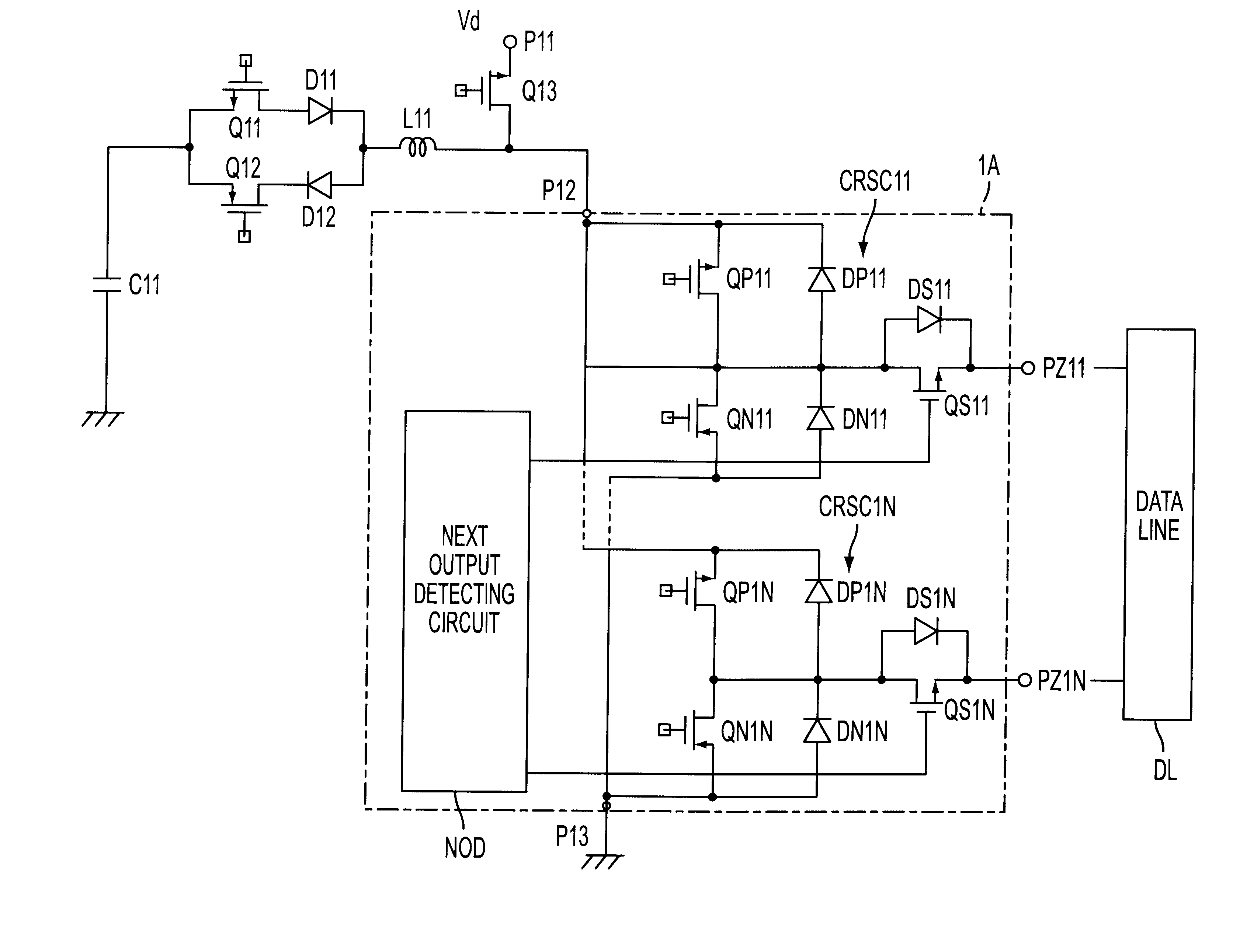
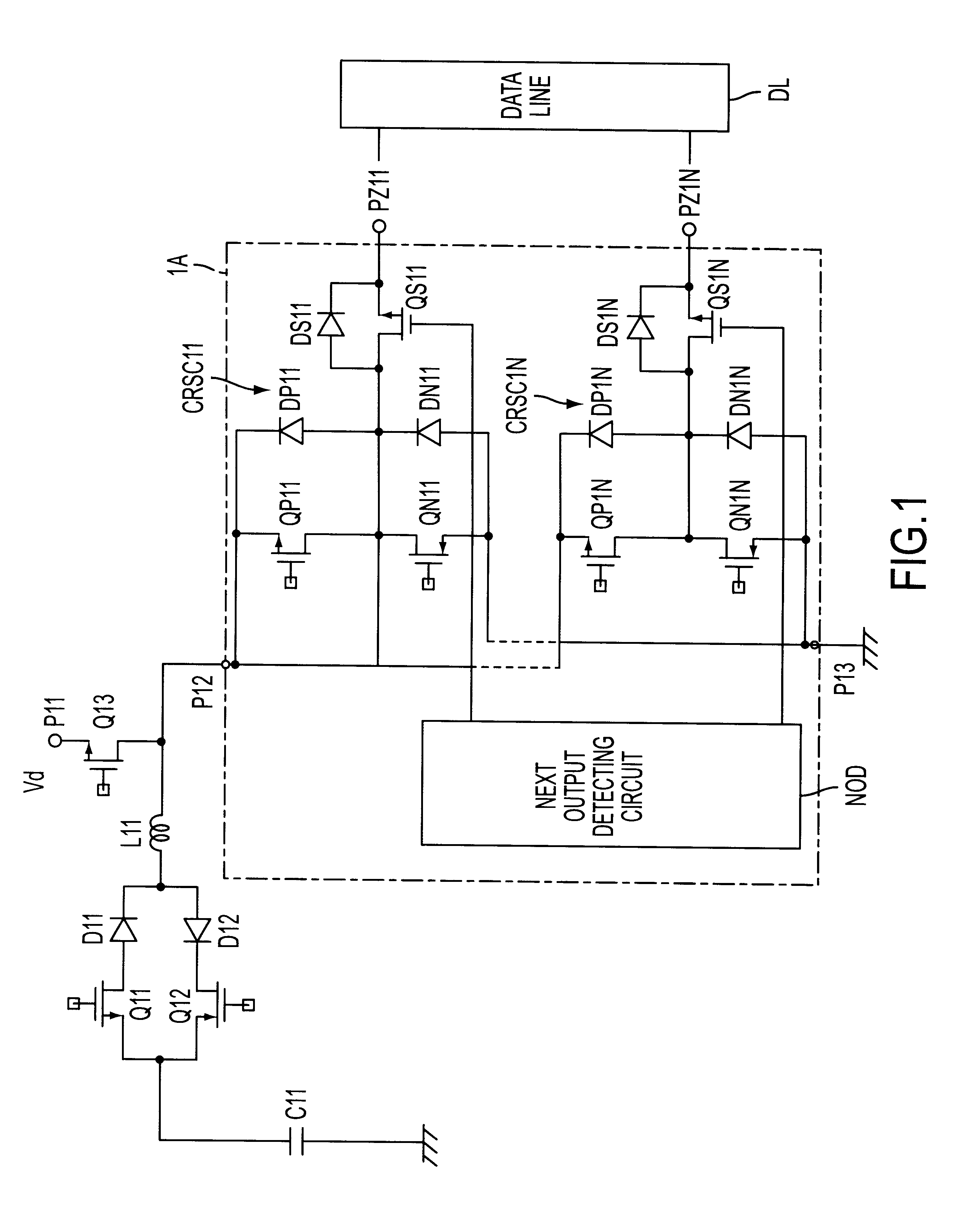
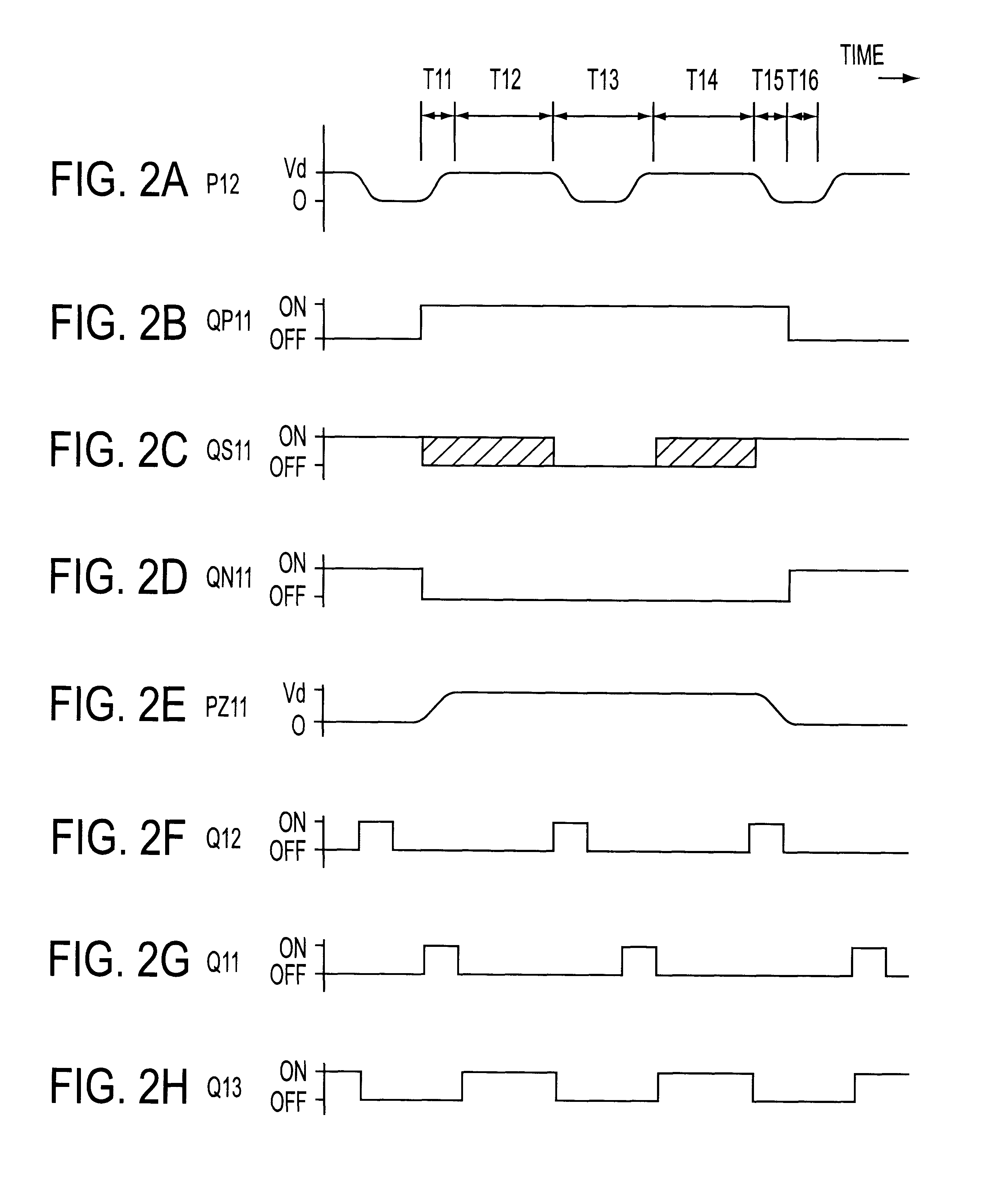
Embodiments of the data line drive circuit of the present invention will be described in detail with reference to the drawings. In this embodiment, FETs are used as switches for turning on or off a high voltage. Any diode which makes use of the parasitic effect of FET will be referred to as parasitic diodes. The configuration of the data line drive circuit of the first embodiment is illustrated in FIG. 1. In the drawing, a reference P11 denotes a terminal for applying a d.c. voltage having a data voltage Vd; P12 denotes a terminal for inputting a data voltage of an integrated circuit 1A used as the data line drive circuit; and P13 denotes a grounded terminal of the integrated circuit 1A used as the data line drive circuit; and P13 denotes a grounded terminal of the integrated circuit 1A. Q13 denotes a P channel FET which serves as a switch which is activated on application of the data voltage. C11 denotes a capacitor for recovering the charge; L11 a coil for recovering the charge; D...

second embodiment

A second embodiment of the data line drive circuit of the present invention will be described in detail with reference to FIGS. 3 and 4. FIG. 3 shows the configuration of the data line drive circuit of the present invention. In the drawings, a reference P21 denotes a terminal for applying a d.c. voltage of the data voltage Vd; P22 a terminal for inputting the data voltage of the integrate circuit 2A which serves as the data line drive circuit; P23 a grounded terminal of the integrated circuit 2A; PZ21 to PZ2N denote output terminals which are connected to the data lines DL. QN21 to QN2N denote N channel FETs and QP21 to QP2N denote P channel FETs. These elements constitute a data voltage applying switch unit for applying the data voltage on the data lines DL which are connected to the output terminals PZ21 to PZ2N. Q21 and Q23 denote P channel FETs which constitute a data voltage applying switch and charge recovering switch, respectively. Q22 and Q24 denotes N channel FETs, which co...

third embodiment

the data line drive circuit of the present invention will be described with reference to FIGS. 5 and 6. The third embodiment is a modification of the second embodiment in which the recovery of the charge on the data lines is conducted simultaneously with the reuse of the charge so that the time required for conducting each operation is reduced to a half of the time. The configuration of the data drive circuit according to the embodiment of the present invention is shown in FIG. 5. In the drawing, reference P31 denotes a terminal for a d.c. voltage of a data voltage Vd; P32 denotes a terminal for inputting a data voltage of the integrated circuit 3A which serves as the data line drive circuit; P33 denotes a grounded terminal of the integrated circuit 3A. References QP31 to QP3N denote P channel FETs; QN31 to QN3N denote N channel FETs. These elements (pair of QP3N and QN3N) constitute a switch unit for applying a data voltage on each of the data lines DL. References Q31, Q33 and Q35 ...


PUM


Abstract

For saving power by recovery and reuse of charge on data lines of a matrix display panel, a data line drive device, has a simplified circuit configuration. The device comprises a matrix display panel having a plurality of data lines DL; a data line drive circuit 1A for driving said data lines DL, including a plurality of switch units QP1i, QN1i (i=1 to N) interposed between a data voltage applying terminal P12 and each of said data lines DL; electrostatic charge storage means C11, L11 for storing electrostatic charge on said data lines, which is connected to said data drive circuit 1A; and a switch QS1i for recovering the charge, having a parasitic diode DS1i which is interposed between said data line drive circuit 1A and each of said data lines, said charge recovering switch QS1i being brought into a conductive state when the charge on the data lines is recovered to said charge storing means C11, L11.

Description

The present invention relates to a matrix display panel such as a plasma display, liquid crystal panel, electroluminescent panel and the like, and in particular to a data line drive device for driving the matrix of the display panel.RELATED ARTTypical matrix display panel include plasma display, liquid crystal panel, electroluminescent panel and the like. The present invention will be described with reference to a plasma display panel. Referring now to FIG. 7, there are shown only the lines of the plasma display panel. PDP denotes a plasma display panel. First and second insulating substrates 11 and 12 which will be described hereafter are sandwiched at a seal portion along the periphery of the panel so that a space therebetween is filled with a discharge gas. S.sub.1, S.sub.2, . . . , Sm denote scanning lines. Ca.sub.1, Ca.sub.2, Cam denote hold lines. Da.sub.1, Da.sub.2, Dam-1, Dan denote data lines. SDR denotes a circuit driving the scanning lines. CDR denotes a circuit driving t...

Claims


Application Information

Patent Timeline
IPC IPC(8): G09G3/28H03K19/00G09G3/296G09G3/20
CPCG09G3/2965H03K19/0019G09G3/293G09G2310/0275
Inventor SHIRASAWA, HIROSHI
Owner PANASONIC CORP
Why Eureka
Try Eureka