
Method to increase the clear ratio of capacitor silicon nitride to improve the threshold voltage uniformity

a technology of silicon nitride and clear ratio, which is applied in the direction of semiconductor devices, diodes, electrical apparatus, etc., can solve problems such as threshold voltage (vt) uniformity problems

Inactive Publication Date: 2001-06-26
TAIWAN SEMICON MFG CO LTD
View PDF6 Cites 15 Cited by
  • Summary
  • Abstract
  • Description
  • Claims
  • Application Information

AI Technical Summary

Benefits of technology

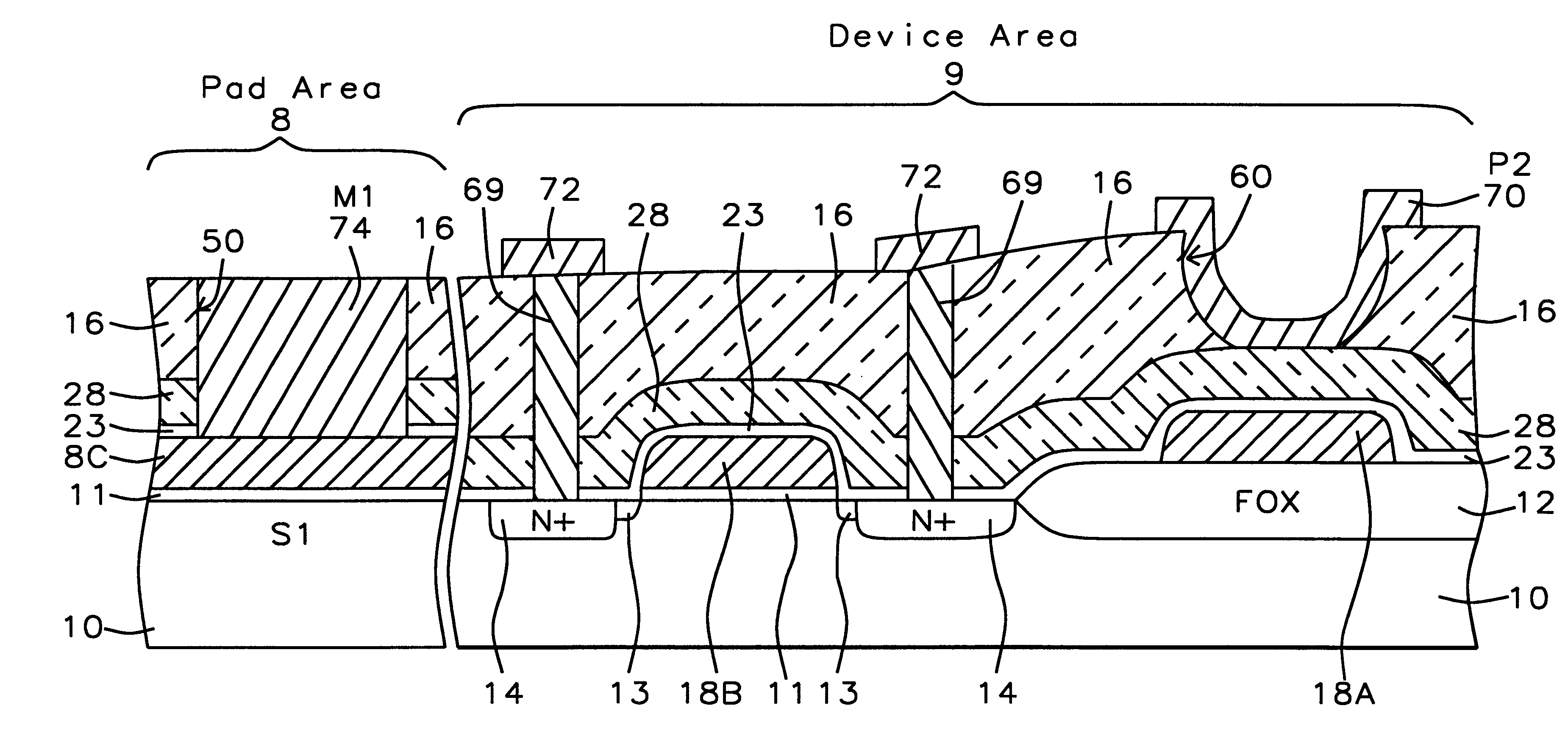
It is an object of the present invention to provide a method for fabricating a pad contact and a capacitor where the SiN over the poly-1 in the pad contact is removed to make She VT more uniform.
It is an object of the present invention to provide a method for fabricating a scribe area and a capacitor where the SiN over the poly-1 in the scribe area is removed to make the VT more uniform.
The inventors have found that threshold voltage (Vt or VT) uniformity is improved when the clear out ratio (area of SiN removed / total area of SiN on whole wafer) is between 1.0584% and 99% and more preferably greater than 1.06%. Uniformity of long channel VT-N was improved when we modify the pad structure of PCM to increase the clear out ratio of capacitor Si.sub.3 N.sub.4 to 1.0584%.

Problems solved by technology

The inventors have found that the SiN over the polysilicon bottom plate causes Threshold voltage (Vt) uniformity problems.

Method used


Image

  • Method to increase the clear ratio of capacitor silicon nitride to improve the threshold voltage uniformity
  • Method to increase the clear ratio of capacitor silicon nitride to improve the threshold voltage uniformity
  • Method to increase the clear ratio of capacitor silicon nitride to improve the threshold voltage uniformity

Examples


second embodiment (

The second embodiment (remove SiN on testsite pads)can be summarized as comprising:

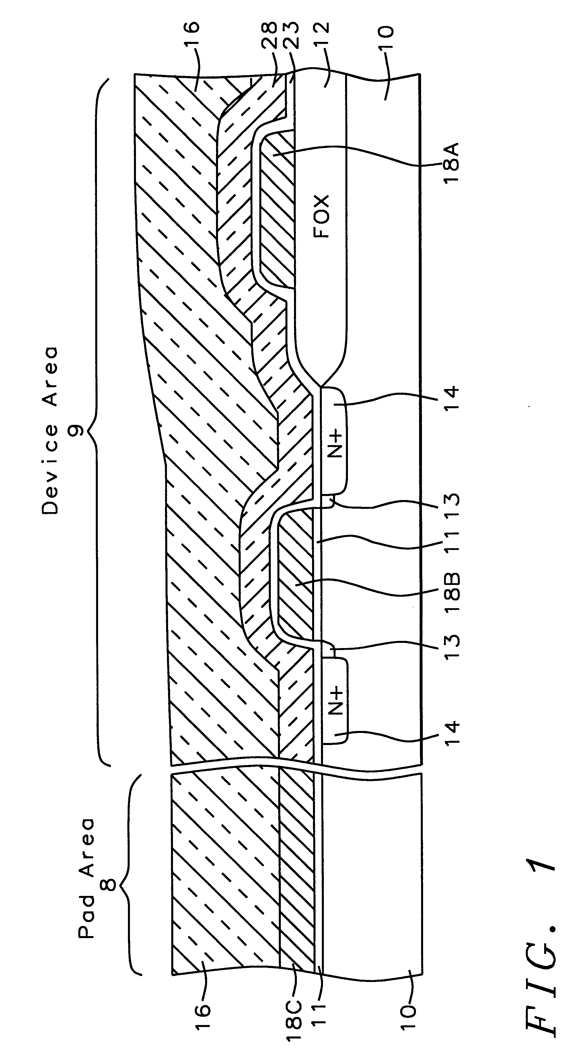
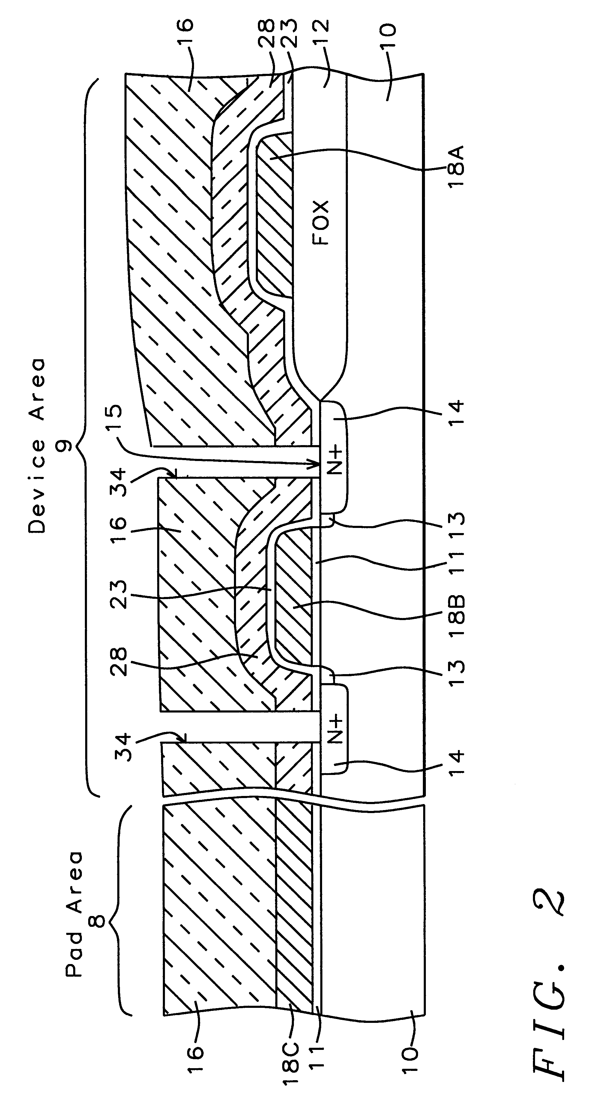
a) See FIG. 8 and FIG. 1--providing a substrate 10 having chip areas 100 and scribe areas 130; a testsite area 135 in the scribe areas 130; the testsite areas having testside pad areas 137; the chip areas 100 having pad areas 8;

b) providing field oxide isolation regions 12 in the substrate; providing contact regions 14 in the chip areas in the silicon substrate 10;

c) forming a first polysilicon layer over the substrate;

d) patterning the first polysilicon layer to define first polysilicon capacitor plates 18A on the field oxide isolation regions; and gate electrodes 18B over the substrate; and polysilicon pads 18C over the testsite area 137;

e) forming a IPO layer of insulator dielectric over the substrate covering the first polysilicon capacitor plates and gate electrodes 18B and polysilicon pads 18C;

f) forming a silicon nitride layer 28 over the IPO layer;

g) forming an interlevel dielectric (ILD) laye...

third embodiment

IV. Third Embodiment--Remove SiN 28 Over the Scribe Lines 130

The third preferred embodiment of the invention removes the silicon nitride layer from over the scribe area. The third preferred embodiment most preferably removes the SiN layer and ILD layer from the entire scribe area 130. FIG. 7 shows a top plan view of a wafer 10 having chips 100 and scribe lines 130 between the chips 100.

FIG. 9 shows a cross sectional view with the ILD 16 and SIN layers 28 removed from the scribe area 130. The PCM testsite area 135 is shown with an example of a MOSFET 140 which is used to test the threshold voltage (VT).

A dark tone scribe area has the interlevel dielectric (ILD) layer and SiN layer remaining during the contact etch. The invention's clear tone scribe area has the interlevel dielectric (ILD) 16 and the SiN layer 28 etched away during the contact etch (as described above for the first embodiment). The process for removing the SiN layer over the scribe area is the same as described above ...


PUM


Abstract

A method to remove the silicon nitride capacitor dielectric layer from over the poly-1 layer on portions of the wafer including non-capacitor areas such as the pad contact area, process control monitor (PCM) testsite areas and scribe line areas. By removing the silicon nitride, H2 can penetrate to the polysilicon and thereby increase the uniformity of the VT. In a first embodiment of the invention, the silicon nitride capacitor dielectric layer is etched away from over the poly-1 layer in the pad area. The removal of the SiN layer allows H2 to penetrate into the poly-1 layer and improve the threshold voltage (VT). Uniformity of long channel VT-N was improved when we modify the pad struture of PCM to increase the clear out ratio of capacitor Si3N4 to 1.0584%. In a second embodiment of the invention, the silicon nitride capacitor dielectric is etched away from over the poly-1 layer in the process control monitor (PCM) testsite area between the chips. In a third embodiment of the invention, the silicon nitride capacitor dielectric is etched away from over the poly-1 layer in the scribe area between the between the chips.

Description

BACKGROUND OF INVENTION1. Field of the InventionThis invention relates generally to fabrication of capacitors for semiconductor devices and more particularly to the fabrication of a capacitors and pad contacts for an analog integrated circuit device.2. Description of the Prior ArtIn the fabrication of combined analog and digital integrated circuits it is common to form capacitors over field oxide regions and form MOS FET near by. For the inventors to improve the capacitor performance, higher dielectric constant capacitor SiN (silicon nitride) is deposited over the bottom storage electrode (poly-1) layer and before the interlevel dielectric (ILD).The inventors have found that the SiN over the polysilicon bottom plate causes Threshold voltage (Vt) uniformity problems.The importance of overcoming the various deficiencies noted above is evidenced by the extensive technological development directed to the subject, as documented by the relevant patent and technical literature. The closest...

Claims


Application Information

Patent Timeline
Patent Type & Authority Patents(United States)
IPC IPC(8): H01L27/06H01L21/70H01L21/8242H10B12/00
CPCH01L27/0629H01L27/1085H01L27/10894H10B12/03H10B12/09
Inventor KU, SHU-MEIWU, LIN-JUNE
Owner TAIWAN SEMICON MFG CO LTD
Learn More