
Method of producing semiconductor thin film and method of producing solar cell using same

a technology of semiconductor thin film and solar cell, which is applied in the direction of crystal growth process, after-treatment details, transportation and packaging, etc., can solve the problems of reducing productivity, peeling with a large force, and damaging the semiconductor thin film

Inactive Publication Date: 2001-07-10
CANON KK
View PDF14 Cites 81 Cited by
  • Summary
  • Abstract
  • Description
  • Claims
  • Application Information

AI Technical Summary

Benefits of technology

Another object of the present invention is to provide a method for holding the substrate without contamination.
Further, the present invention provides a method of producing a semiconductor thin film comprising peeling a semiconductor thin film formed on a substrate away from the substrate, wherein the peeling is carried out after the substrate is secured on a substrate support member without an adhesive. According to this method, the substrate can be secured without contamination. The substrate is preferably held by vacuum suction, by electrostatic suction (adhesion), or by a securing claw.
The present invention also provides a method of producing a solar cell comprising forming a separation layer on a substrate and forming a semiconductor thin film having a semiconductor layer of a first conductivity type and a semiconductor layer of a second conductivity type on the separation layer, bonding a light-transmitting film onto the semiconductor thin film with a light-transmitting adhesive, exerting an external force on the light-transmitting film to peel the semiconductor thin film away from the substrate, and forming an electrode on a back surface of the semiconductor thin film thus peeled. Further, the present invention provides a method of producing a solar cell comprising forming a separation layer on a substrate and forming a semiconductor thin film of a first conductivity type on the separation layer, bonding a light-transmitting film onto the semiconductor thin film of the first conductivity type with a light-transmitting adhesive, exerting an external force on the light-transmitting film to peel the semiconductor thin film of the first conductivity type away from the substrate, forming a semiconductor thin film of a second conductivity type on a back surface of the first semiconductor thin film thus peeled, and forming an electrode on the semiconductor thin film of the second conductivity type. According to the above methods, the solar cell can be produced through simple steps.

Problems solved by technology

Therefore, considerable force is necessary for the peeling.
This could result in damaging the semiconductor thin film.
In addition, the above techniques require a step of applying and curing the adhesive for securing the substrate to the plate or to the jig, which decreases productivity.

Method used


Image

  • Method of producing semiconductor thin film and method of producing solar cell using same
  • Method of producing semiconductor thin film and method of producing solar cell using same
  • Method of producing semiconductor thin film and method of producing solar cell using same

Examples


example 2

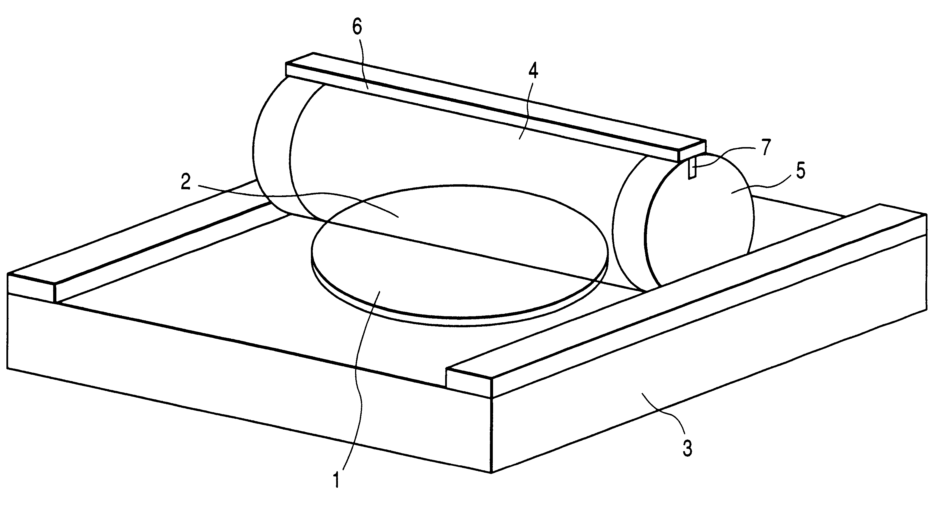
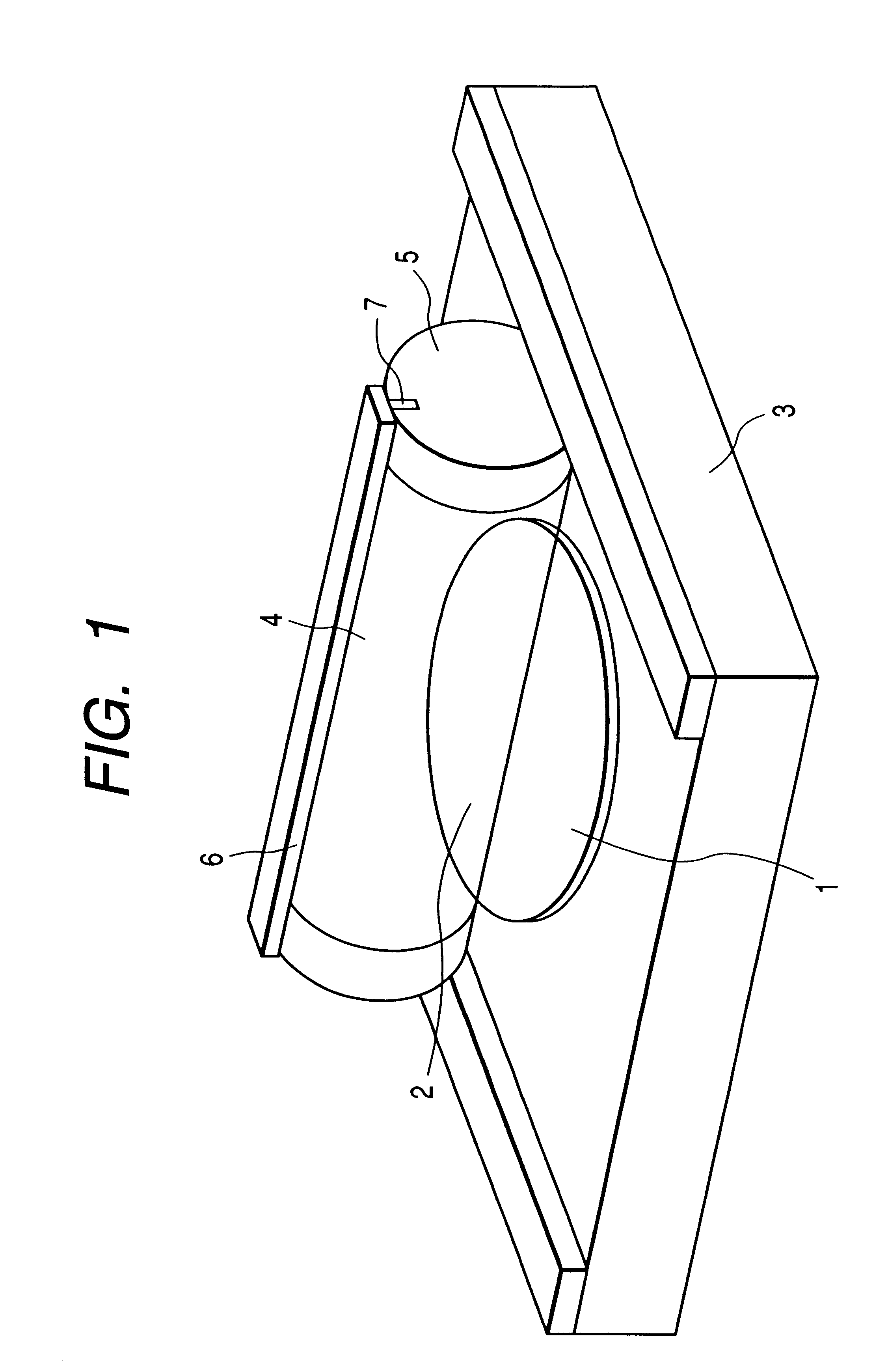
Next described referring to FIG. 9 is another example of applying the method of producing a semiconductor thin film according to the present invention to the production of a solar cell. FIG. 9 is a schematic, sectional view for explaining the application example to production of a solar cell using an opaque material for the film 4. In the present example, the p.sup.- single-crystal silicon substrate 1 is first anodized to form the porous layer 16 and then it is subjected to hydrogen annealing. After that, the n.sup.+ silicon layer and p.sup.- silicon layer are epitaxially grown thereon. Then a p.sup.+ silicon layer is formed by epitaxial growth or by diffusion of a p-type dopant from the surface of the p.sup.- silicon layer. Then a film electrically conductive at least in the surface, i.e., electroconductive film 4, is bonded to the surface. The electroconductive film 4 can be obtained by sputtering or evaporating a metal such as aluminum or the like on a resin film or a thin film o...


PUM

PropertyMeasurementUnit
Forceaaaaaaaaaa
Poweraaaaaaaaaa
Flexibilityaaaaaaaaaa

Abstract

Provided is a method of producing a semiconductor thin film wherein while a semiconductor thin film formed on a substrate is supported on a curved surface of a support member having the curved surface, the support member is rotated, thereby peeling the semiconductor thin film away from the substrate. Also provided is a method of producing a semiconductor thin film having the step of peeling a semiconductor thin film formed on a substrate away from the substrate, wherein the peeling step is carried out after the substrate is secured on a substrate support member without an adhesive. These provide the method of peeling the semiconductor thin film away from the substrate without damage and the method of holding the substrate without contamination.

Description

1. Field of the InventionThe present invention relates to a method of producing a semiconductor thin film and, more particularly, to a method of peeling a semiconductor thin film and a method of producing a solar cell using the semiconductor thin film.2. Related Background ArtKnown technology includes the formation of a semiconductor thin film through a peeling layer such as a porous layer or the like on a semiconductor substrate and thereafter peeling the semiconductor thin film away from the semiconductor substrate. Specific peeling methods include etching methods and mechanical peeling methods with application of external force.As an example of the latter, Japanese Patent Application Laid-Open No. 7-302889 (CANON K.K.) describes the technique of forming a porous layer on a surface of a first silicon wafer, thereafter forming an epitaxial silicon layer thereon, bonding a second silicon wafer to the epitaxial silicon layer, further bonding plates to the respective silicon wafers, a...

Claims


Application Information

Patent Timeline
IPC IPC(8): C23C16/00C23C16/01C30B33/00H01L21/762H01L21/70H01L31/18H01L31/04
CPCC23C16/01C30B33/00H01L21/76251H01L31/1892C30B29/60Y02E10/50Y10T156/1179Y10S156/93Y10S156/942Y10T156/1978
Inventor MIZUTANI, MASAKITANIKAWA, ISAONAKAGAWA, KATSUMISHOJI, TATSUMIUKIYO, NORITAKAIWASAKI, YUKIKO
Owner CANON KK
Features
  • Generate Ideas
  • Intellectual Property
  • Life Sciences
  • Materials
  • Tech Scout
  • Unparalleled Data Quality
  • Higher Quality Content
  • 60% Fewer Hallucinations
Learn More