Method and apparatus for clock gated logic circuits to reduce electric power consumption

Inactive Publication Date: 2001-08-07
KK TOSHIBA
View PDF2 Cites 52 Cited by
  • Summary
  • Abstract
  • Description
  • Claims
  • Application Information

AI Technical Summary

Problems solved by technology

In recent years, the integration and the chip size of LSIs have dramatically increased to require much power consumption.
It is known that the power consumption is increased when the clock signal supplied to the flip-flops rises up or falls down in the operation of the logic circuit of this kind.
However, unnecessary power consumption occurs when there is no need for loading data to flip-flops, since the clock signal is continuously input to the flip-flops irrespective of existence of data to be loaded.
However, in accordance with the prior art clock gating circuit designing technique, any proposals for generating appropriate enable signals have not been made from the view point of the power saving efficiency.
For this reason, it is not confirmed that the enable signals as used are appropriate for the power saving efficiency so that it, is often the case that the clock gating circuit designing technique has been conducted with inefficient enable signals.
On the other hand, while the frequency of the clock signal as supplied to the circuits integrated within an LSI chip has been drastically increased, the electric power consumption is also proportionally increased along therewith resulting in difficult problems associated.
More specifically speaking, as a result of the increased electric power consumption, the heat as generated tends

Method used


Image

  • Method and apparatus for clock gated logic circuits to reduce electric power consumption
  • Method and apparatus for clock gated logic circuits to reduce electric power consumption
  • Method and apparatus for clock gated logic circuits to reduce electric power consumption

Examples


first embodiment

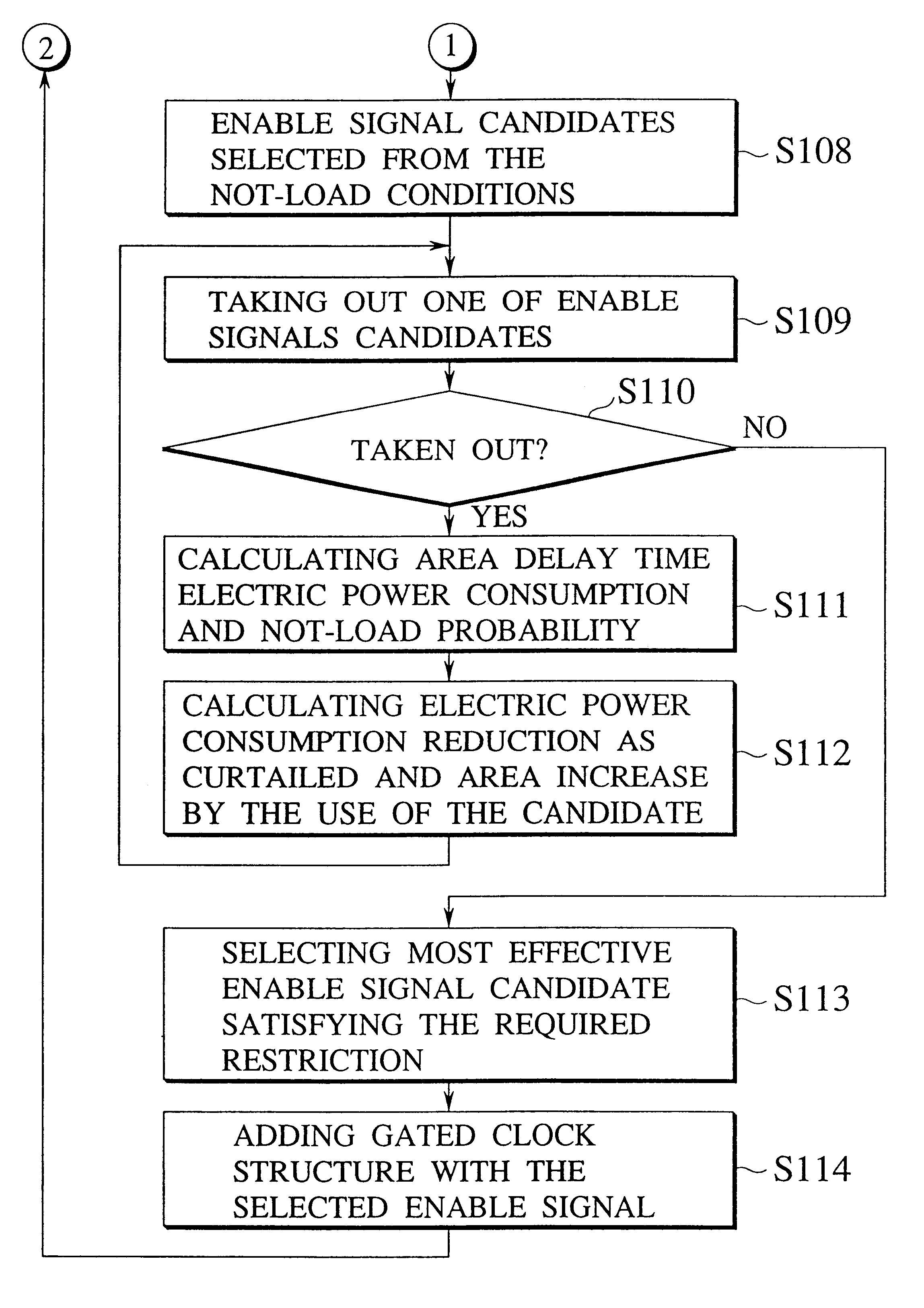
Referring now to the accompanying drawings, several embodiments of a clock supplying circuit and an enable buffer cell, and a computer aided design system and method for clock gated logic circuits, an enable buffer cell, and a computer program embodied on a computer-readable medium for designing clock gated logic circuits in accordance with the present invention will be explained in details. FIG. 7 is a function block diagram of a computer aided design system for clock gated logic circuits regarding the present invention.

For designing a clock gated layout on a logic circuit, this computer aided design system for clock gated logic circuits comprises a circuit information storing section 1, a non-load condition input section 2, a non-load condition extraction section 3, an enable signal candidate generation section 4 and, an area / delay / electric power analysis section 5, an enable signal candidate information storing section 6, design restriction input section 7, an enable signal selec...

second embodiment

FIG. 17 is a table showing exemplary information of non-load conditions as input through the non-load condition input section 2 in accordance with the present invention.

Explained in this embodiment of the present invention is the case that the non-load conditions as illustrated in FIG. 17 are input through the non-load condition input section 2 in the same configuration as illustrated in FIG. 7 to FIG. 10. In accordance with this embodiment of the present invention in which non-load conditions are additionally input through the non-load condition input section 2, it is possible to take into consideration the non-load conditions which can not be extracted by the non-load condition extraction section 3 and the "don't care" conditions direct1y extracted from the logic circuit, so that more appropriate enable signals can be generated as compared to the first embodiment. Meanwhile, information stored in the circuit information storing section 1 is similar to that as illustrated in FIGS. ...

third embodiment

Hereinbelow, a third embodiment will be explained. Explained in this embodiment of the present invention is the case that, when an enable signal is selected among from the enable signal candidates by the enable signal selection section 8, a user of the system is provided with the enable signal candidate information in the form of a graph or a table on the CRT in order to enable him to select appropriate enable signals in the same configuration as illustrated in FIG. 7 to FIG. 10.

In this embodiment of the present invention, information of the second embodiment as illustrated in FIG. 18 is stored in the enable signal candidate information storing section 6. Namely, a graph as illustrated in FIG. 20 is displayed in the CRT 19 with an ordinate indicative of the electric power consumption reduction and an abscissa indicative of the area as increased by introduction of the respective one of the eight enable signal candidates. The user can select an enable signal by pointing one of the ena...


PUM


Abstract

A computer aided design technique for clock gated logic circuits effective to reduce the electric power consumption is disclosed. The computer aided design for clock gated logic circuits is conducted by extracting, by the use of information about a clock gated logic circuit under the design, a halt condition under which a clocked circuit driven by a clock signal can halt with no clock signal supplied, generating enable signal candidates, from said halt condition, which can be used as enable signals in the clock gated logic circuit, analyzing the clock gated logic circuit in order to obtain information about a delay time of signal transmission and electric power consumption reduction if respective one of enable signal candidates is used as an enable signal of a clock gating circuit inserted in the clock gated logic circuit under the design, storing enable signal candidate information including the result of the analysis conducted by said analysis step in a information store means, selecting an appropriate one of the enable signal candidates which satisfy given restrictions regarding a delay time of signal transmission in the clock gated logic circuit under the design, by the use of said enable signal candidate information; and adding the clock gating circuit activated with the enable signal as selected by said enable signal selection step to the clock gated logic circuit under the design.

Description

1. Field of the InventionThe present invention is related to a gated clock design technique by the use of a computer, and more particularly related to a clock supplying circuit and an enable buffer cell, and a computer aided design system and method for clock gated logic circuits and design method thereof and an enable buffer cell.2. Description of the Prior ArtIn recent years, the integration and the chip size of LSIs have dramatically increased to require much power consumption. The gated clock design technique has been developed for the purpose of obtaining the logic circuit designs with low electric power consumption.The procedure of modifying logic circuits by means of the gated clock design technique is called as "clock gating" in the following explanation. First, the gated clock design as mentioned above will be briefly explained.FIG. 1 is a partial circuit diagram showing a clocked logic circuit which has not been clock gated. In the same figure, the reference symbols FF0,FF...

Claims


Application Information

Patent Timeline
IPC IPC(8): G06F17/50
CPCG06F17/505G06F2217/78G06F30/327G06F2119/06
Inventor MINAMI, FUMIHIROKITAHARA, TAKESHIUSAMI, KIMIYOSHINISHIO, SEIICHI
Owner KK TOSHIBA
Why Eureka
Try Eureka