Very long and highly stable atomic wires, method for making these wires, application in nano-electronics

a technology of atomic wires and wires, applied in the field of manufacturing atomic wires, can solve the problems of thermal instability of the wire obtained, the length of the atomic wire is generally limited to a few tenths of a nanometer, and the method has drawbacks

Inactive Publication Date: 2001-08-14
COMMISSARIAT A LENERGIE ATOMIQUE ET AUX ENERGIES ALTERNATIVES +1
View PDF8 Cites 44 Cited by
  • Summary
  • Abstract
  • Description
  • Claims
  • Application Information

AI Technical Summary

Problems solved by technology

However, this method has drawbacks.
This is because the wires obtained are thermally unstable, because notably of the substrates or adsorbates employed.
In addition, the length of these atomic wires is generally limited to a few tenths of a nanometer, and their distribution over the surface is random and therefore not controllable.
The atomic wires are of poor quality on an atomic scale.
In addition, only a small number of wires can be obtained by this method.
Moreover, this method generally requires a su

Method used


Image

  • Very long and highly stable atomic wires, method for making these wires, application in nano-electronics
  • Very long and highly stable atomic wires, method for making these wires, application in nano-electronics
  • Very long and highly stable atomic wires, method for making these wires, application in nano-electronics

Examples


Embodiment Construction

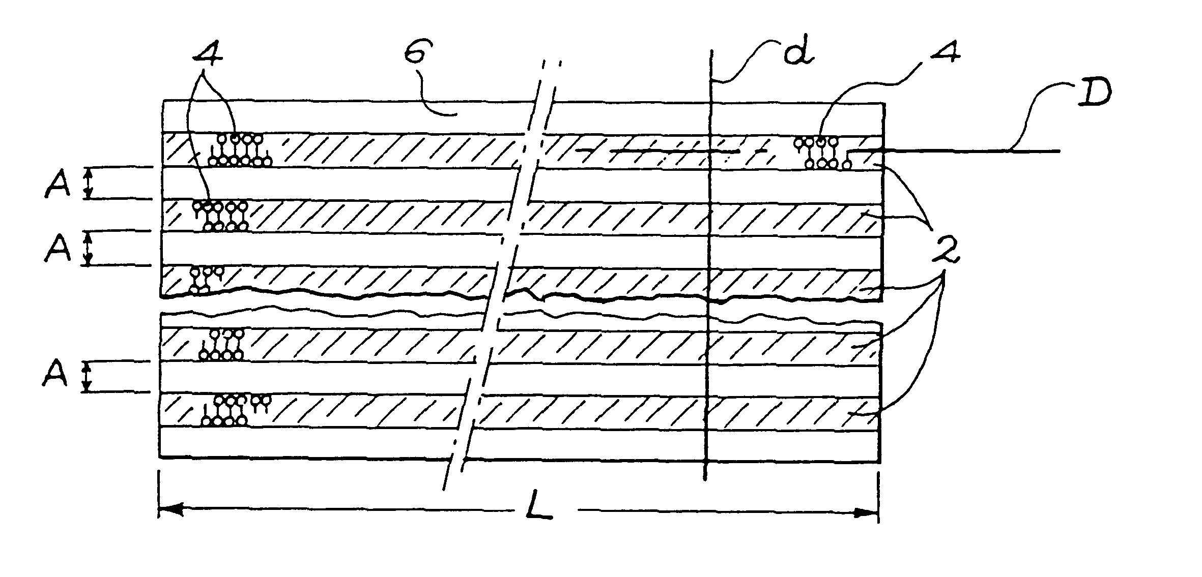
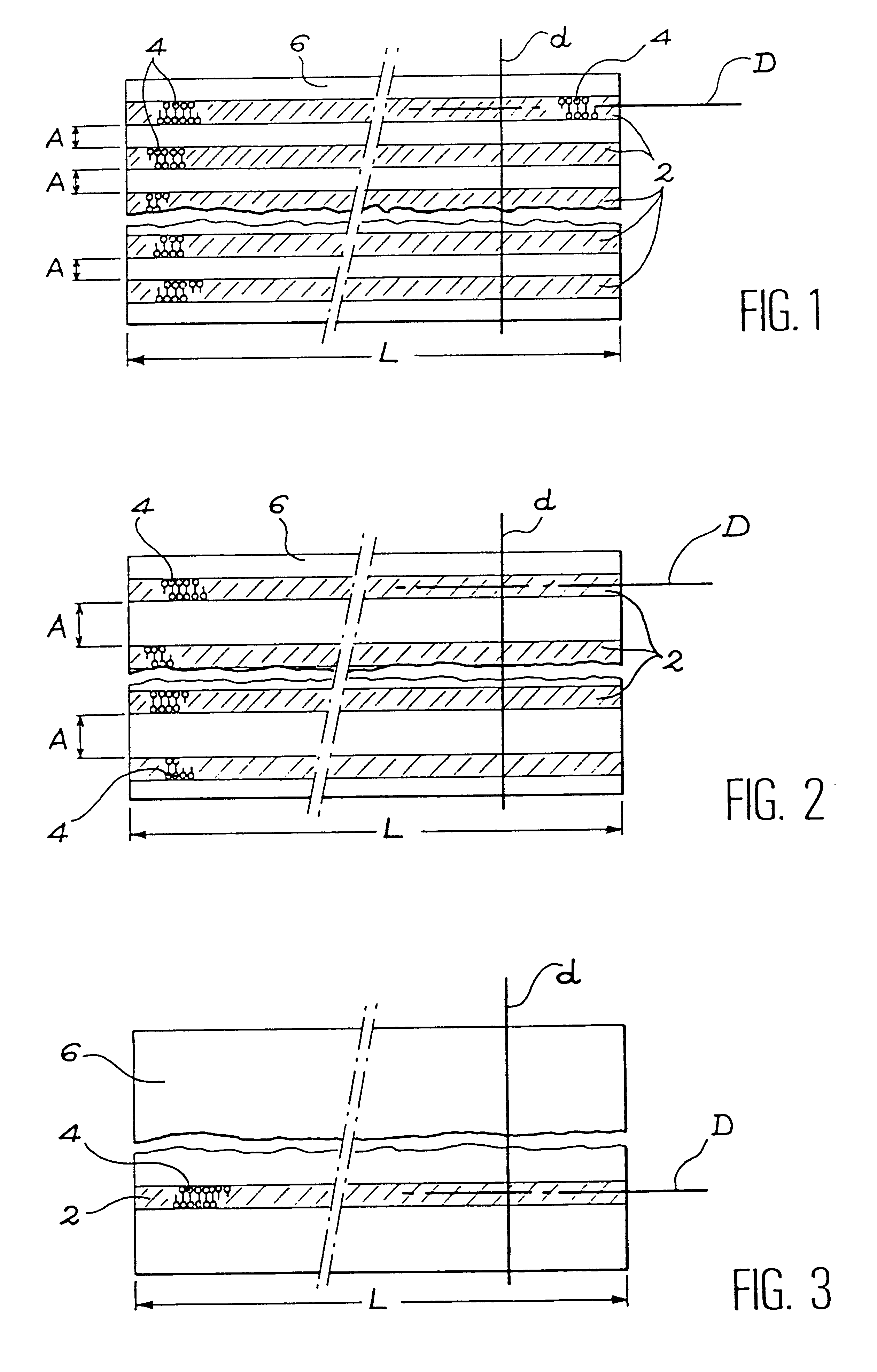
The invention therefore concerns atomic lines or wires of great length, formed on the surface of a silicon carbide substrate.

It is possible to vary the distances between the atomic wires in a controlled fashion, from 1 nm to several millimetres.

This is illustrated schematically in plan view by FIGS. 1 to 3.

In FIGS. 1 and 2, atomic wires 2 can be seen, which are chains of silicon dimers (Si--Si ) referenced 4, are very straight and all have the same direction D.

Their length L is very great (greater than 100 nm) and is limited only by the length of the substrate 6 on which these wires 2 are formed.

These wires are regularly spaced apart from each other.

They extend perpendicularly from the direction d of the dimers.

It is possible to vary the number N of atomic wires with the temperature in order to change from a super-lattice of atomic wires, which are separated from each other by a distance of around a few tenths of a nanometer (FIG. 1), to an assembly of atomic wires which are separat...


PUM

PropertyMeasurementUnit
Thicknessaaaaaaaaaa
Thicknessaaaaaaaaaa
Angleaaaaaaaaaa

Abstract

Atomic wires of great length and great stability are formed on the surface of a SiC substrate as straight chains of dimers of an element chosen from amongst SiC and C. In order to produce same, layers of the element are formed on the surface and the assembly is constructed by means of annealings of the surface provided with the layers. The resulting wires have application to nanoelectronics.

Description

The present invention concerns atomic wires of great length and great stability as well as a method of manufacturing these wires.The invention applies particularly to the field of nano-electronics, optics and micromechanics.PRIOR ARTVarious works have been devoted to the manufacture of atomic wires on metal surfaces or semiconductor surfaces.The formation of atomic wires results from processes bringing into play the structural, dynamic and reactivity properties of solid surfaces on an atomic scale.The problem of manufacturing atomic wires is also closely linked to that of the display of these wires formed by atoms.Because of their sub-nanometric dimensions (less than or equal to 1 nm), the display and inspection of such nano-structures can be achieved only by means of a tunnel-effect microscope.The main known methods of manufacturing atomic wires are indicated below.A first known method consists of a controlled deposition of adsorbate on a solid surface.According to this first known...

Claims


Application Information

Patent Timeline
IPC IPC(8): C30B33/00H01L21/02C30B29/60H01L21/20H01L21/04H01L21/28H01L29/15H01L29/161
CPCB82Y10/00C30B33/00H01L21/02H01L51/0595C30B29/36C30B29/605Y10S977/762Y10T428/265Y10T428/24917Y10S977/712H10K10/701
Inventor DUJARDIN, GERALDMAYNE, ANDREWSEMOND, FABRICESOUKIASSIAN, PATRICK
Owner COMMISSARIAT A LENERGIE ATOMIQUE ET AUX ENERGIES ALTERNATIVES
Why Eureka
Try Eureka