Semiconductor device and method for making pattern data

Inactive Publication Date: 2001-09-11
ADVANCED INTERCONNECT SYST LTD
View PDF13 Cites 13 Cited by
  • Summary
  • Abstract
  • Description
  • Claims
  • Application Information

AI Technical Summary

Problems solved by technology

If the interlayer dielectric layer does not have a flat surface, problems arise in that wiring layers formed on the interlayer dielectric layer may be cut.
As a consequence, a designed shape of a through hole may not be formed or a through hole may not be formed at all.
However, since these distances cannot be made shorter than a minimum processible dimension in manufacturing a semiconductor device, they are set to be a minimum processible dimension in manufacturing a semiconductor device.
On the other hand, the greater the distanc

Method used


Image

  • Semiconductor device and method for making pattern data
  • Semiconductor device and method for making pattern data
  • Semiconductor device and method for making pattern data

Examples


Embodiment Construction

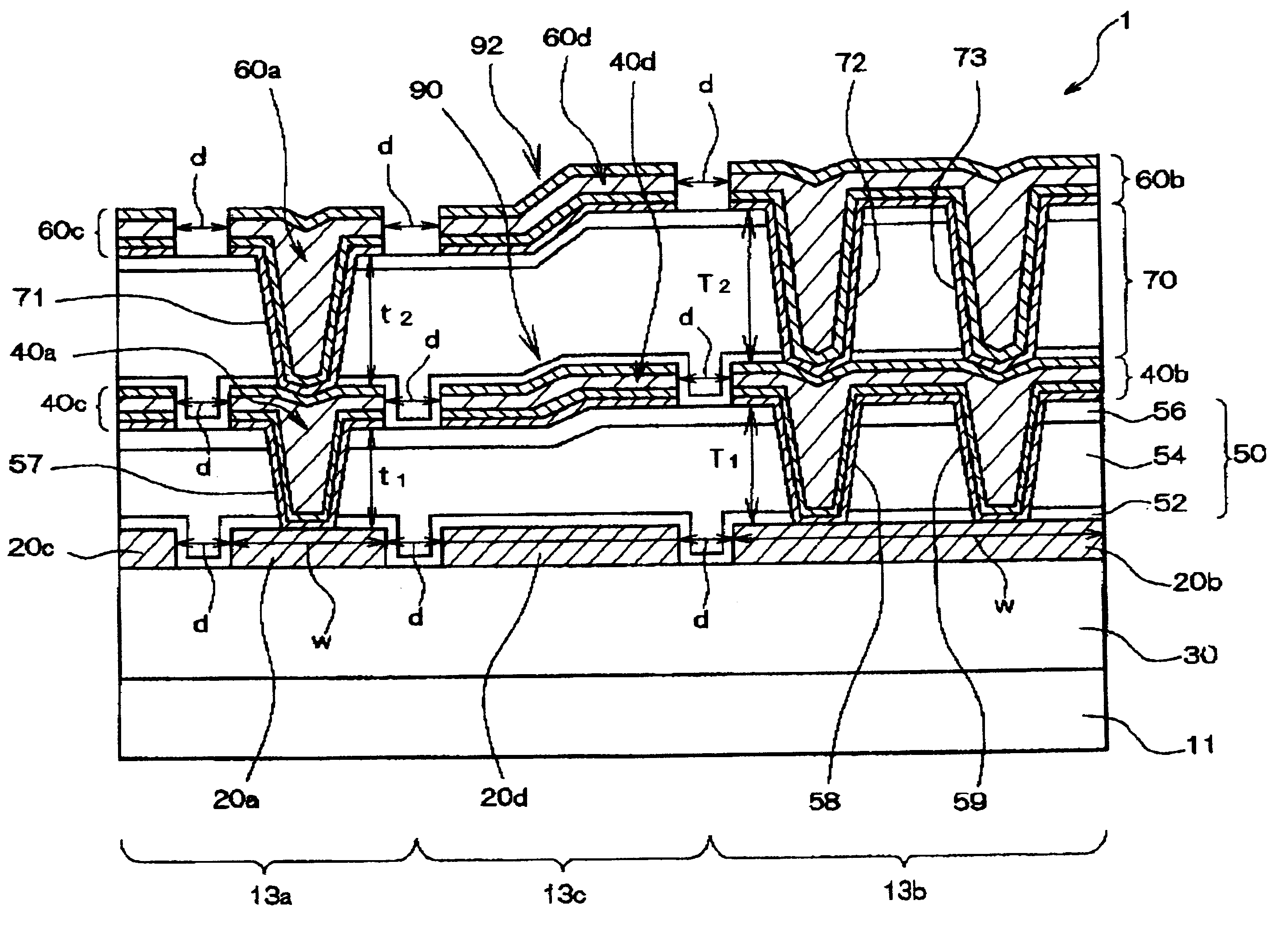
FIG. 1 is a cross-sectional view of a structure of a semiconductor device 1 in accordance with a first embodiment of the present invention. The semiconductor device 1 has a silicon substrate 11, a first metal wiring layer in a first layer (first metal wiring layer 20a and first metal wiring layer 20b), a second metal wiring layer in a second layer (second metal wiring layer 40a and second metal wiring layer 40b), and a third metal wiring layer in a third layer (third metal wiring layer 60a and third metal wiring layer 60b). The structure of the semiconductor device 1 will be described below in greater detail.

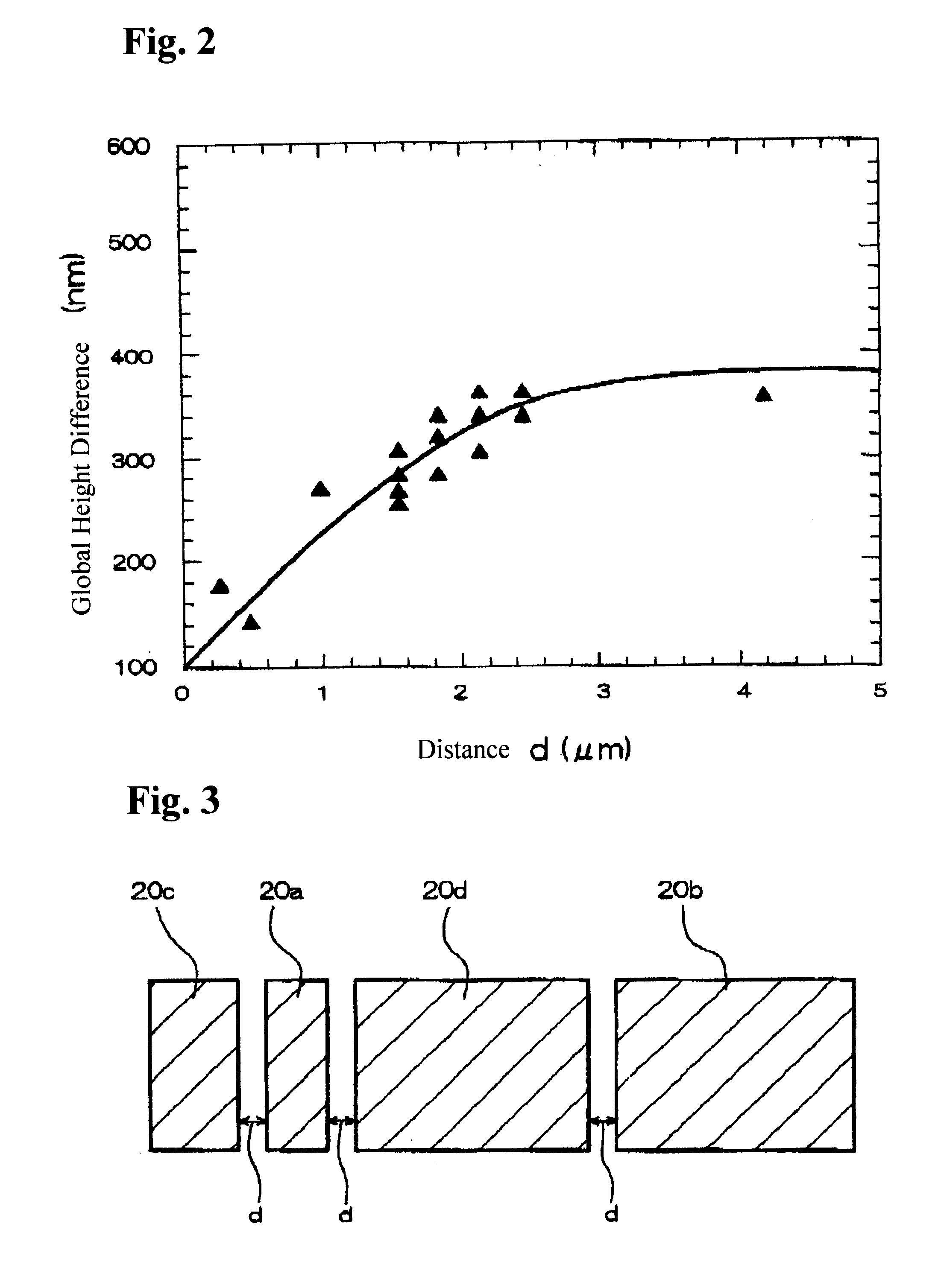
The silicon substrate 11 has a main surface that includes a region 13a, a region 13b and a region 13c.

Metal wiring layers of small patterns are formed in the region 13a. Also, logic circuits and the like (not shown) are formed in the region 13a.

Metal wiring layers of large patterns are formed in the region 13b. Also, power source lines, bonding pads and the like (not shown) are ...


PUM


Abstract

A semiconductor device has a first region, a second region and a border region between the first region and the second region. The semiconductor device has an interlayer dielectric layer, covering at least the first region and the second region. A first wiring layer is located in the first region and defines a relatively small pattern. A second wiring layer is located in the second region and defines a relatively large pattern that is wider than the small pattern. A first dummy pattern is formed in the first region and a second dummy pattern is formed in the border region. The interlayer dielectric layer includes a planarization silicon oxide film. The planarization silicon oxide film is one of a silicon oxide film formed by a polycondensation reaction between a silicon compound and hydrogen peroxide, an organic SOG (Spin On Glass) film an inorganic SOG film and a silicon oxide film formed by reacting an organic silane with ozone or water. The interlayer dielectric layer located over the first wiring layer is thinner than the interlayer dielectric layer located over the second wiring layer such that a global height difference occurs in the border region between the first region and the second region.

Description

1. Field of the InventionThe present invention relates to a semiconductor device and a method for making pattern data.2. Description of Related ArtAn interlayer dielectric layer provided in a semiconductor device has roles in insulating an upper wiring layer from a lower wiring layer, for example. If the interlayer dielectric layer does not have a flat surface, problems arise in that wiring layers formed on the interlayer dielectric layer may be cut.Interlayer dielectric layers having an excellent planarization characteristic includes, for example, a silicon oxide film that is formed by reacting a silicon compound such as silane with hydrogen peroxide through a CVD method. For example, this technology is described in Japanese Laid-open Patent Application HEI 9-102492.Although such a silicon oxide film is used as an interlayer dielectric layer, a global height difference is created along a border between a region in which large patterns of wiring layers are formed and a region in whi...

Claims


Application Information

Patent Timeline
IPC IPC(8): H01L23/532H01L23/52H01L21/02H01L21/70H01L21/768H01L23/522H01L21/3205H01L21/3065H01L21/302H01L21/822H01L27/04
CPCH01L21/32051H01L21/76801H01L21/76804H01L21/76828H01L21/76834H01L21/76843H01L21/76864H01L21/76877H01L23/522H01L23/53223H01L2924/0002Y10S438/926H01L2924/00
Inventor USHIYAMA, FUMIAKI
Owner ADVANCED INTERCONNECT SYST LTD
Why Eureka
Try Eureka