Scaleable low-latency switch for usage in an interconnect structure

a low-latency switch and interconnection structure technology, applied in data switching networks, digital transmission, electrical apparatus, etc., can solve the problems of grid failure, low-latency interconnect that cannot be scaled, bandwidth, etc., and achieve the effect of low latency and highest bandwidth

Inactive Publication Date: 2001-09-11
HEWLETT PACKARD CO +1
View PDF27 Cites 81 Cited by
  • Summary
  • Abstract
  • Description
  • Claims
  • Application Information

AI Technical Summary

Benefits of technology

, one output design, applicable to supercomputers, supplies a highest bandwidth and lowest possibl

Problems solved by technology

A persistent significant unsolved problem in the field of computer science has been the lack of a scalable, low-latency interconnect that sustains high throughput (high cross-sectional bandwidth) under fully loaded conditions.
Existing interconnect designs, such as the banyon, omega and fat-tree networks, multi-level grids, torus and hypercube networks all fail, in various degrees, to scale without limit, support low latency and high throughput when loaded with traffic.
The geometries of these networks were developed by Nineteenth Century mathematicians, and even earlier geometricians, and were never intended to support a message-routing method.
Switches for supercomputer designs are fabricated using expensive silicon fabrication technologies.
The interconnection of nodes is made by multiple, expensive high-speed cables.
Conventional switch technologies have many deficiencies in the support of interconnect structure technologies.
First, no existing switching fabri

Method used


Image

  • Scaleable low-latency switch for usage in an interconnect structure
  • Scaleable low-latency switch for usage in an interconnect structure
  • Scaleable low-latency switch for usage in an interconnect structure

Examples


generalized embodiment

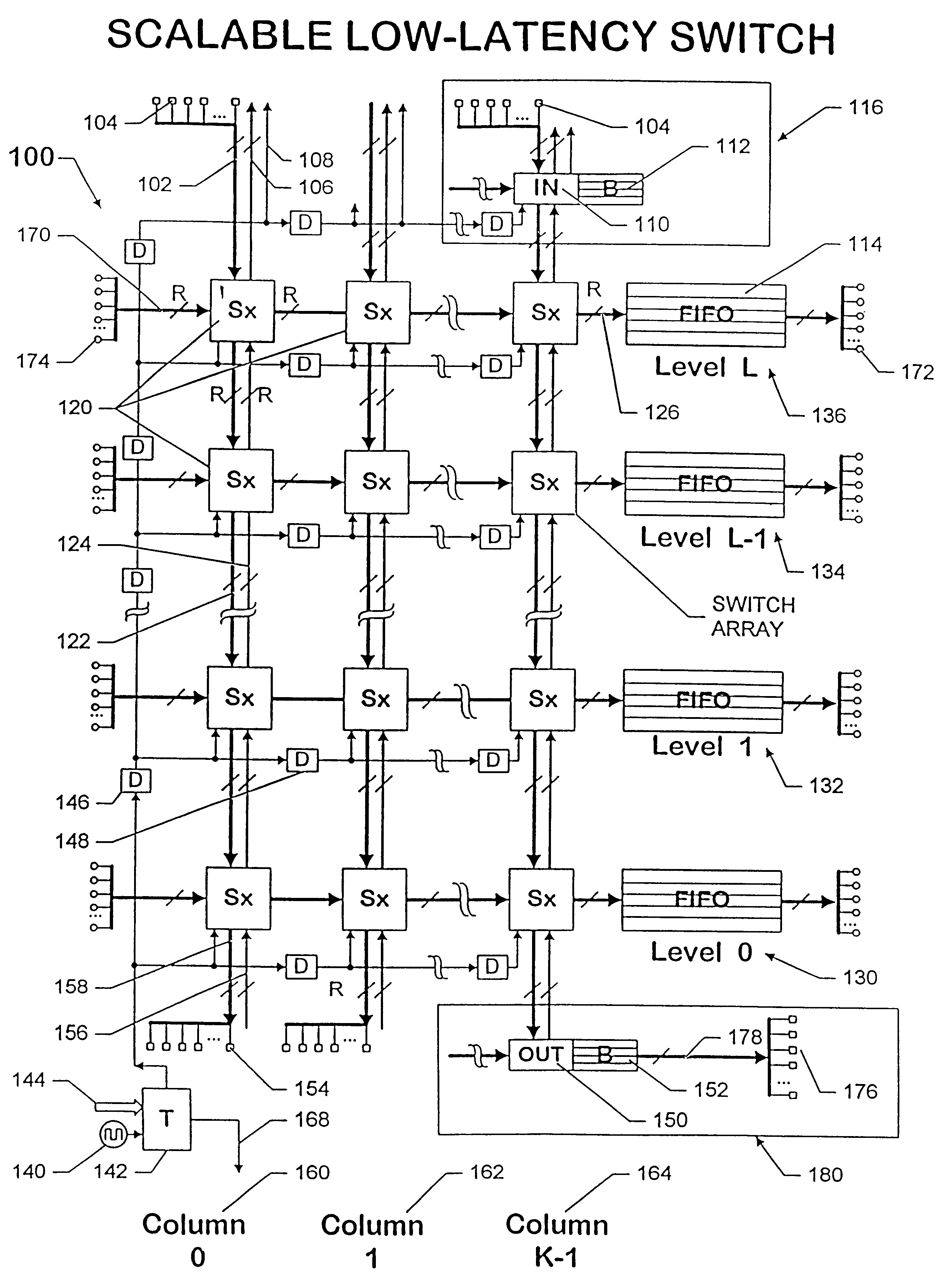
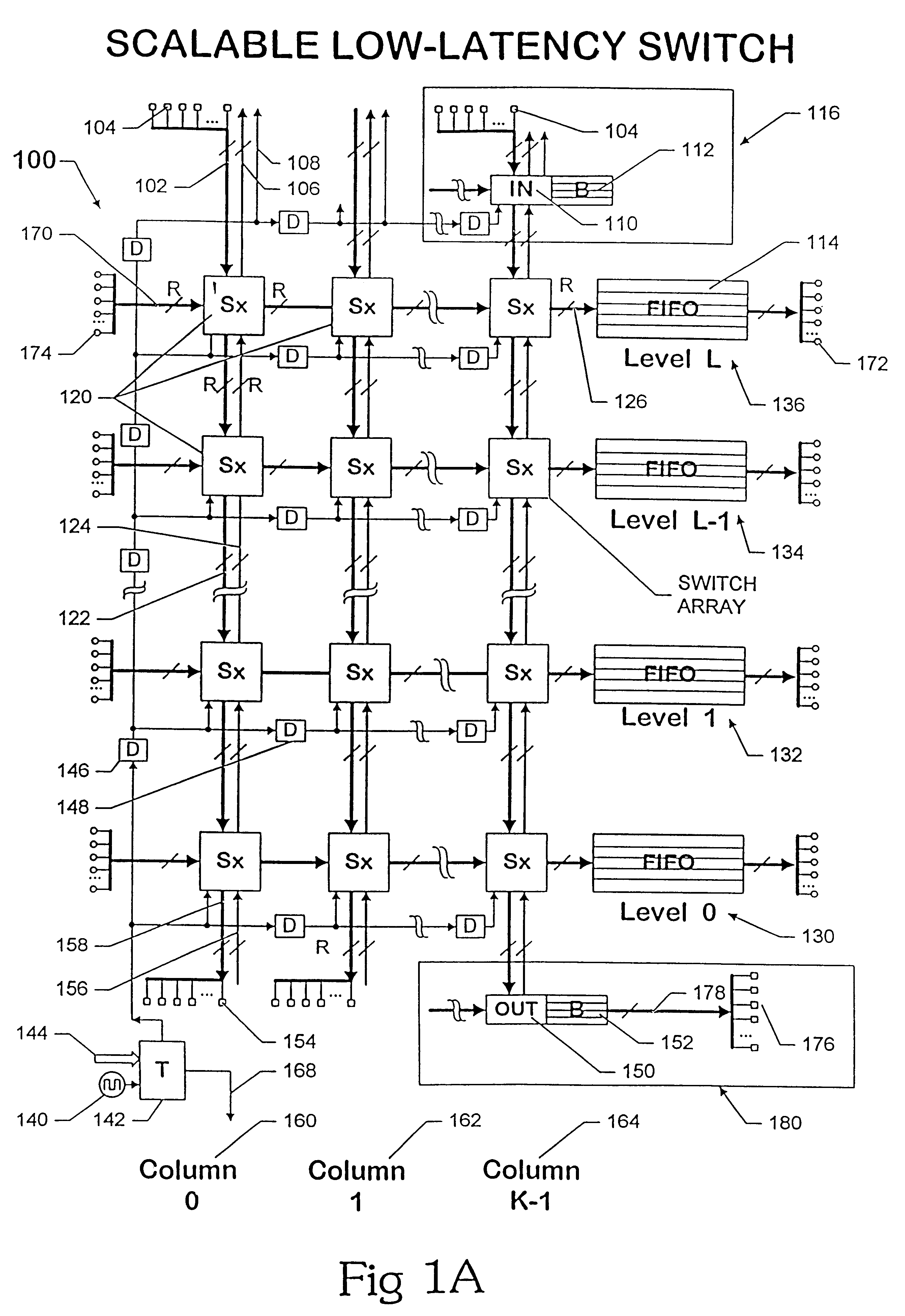
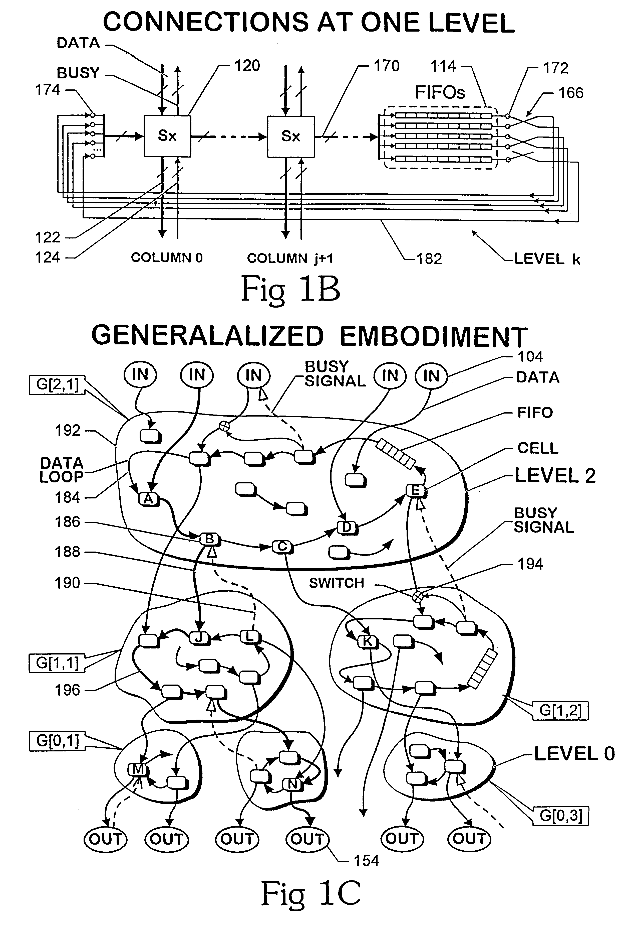
FIG. 1C is a general diagram of Switch 100. In this Figure many components such as control cells and interconnections between control cells are omitted for the sake of clarity. (In this figure the terms "left" and "right" refer to an input path and an output path, respectively, connected to cells at the same level.) Control cells 186 are members of one or more groups of cells at the same level. A group 192 contains one or more data loops 184. In FIG. 1C the top level includes a single group G[2,1] 192, where the first parameter (2) indicates the level and the second parameter (1) indicates a specific group at that level. Cell B 186, within group G[1,1], is connected to other cells that, taken together, form a continuous data loop 184. Data in the form of a message circulating through loop 184 moves through cells A, B, C, D, E, and beyond. In some embodiments where the message length is long, a FIFO is included in data loop 184. A message circulating in a data loop has opportunities ...


PUM


Abstract

A scalable low-latency switch extends the functionality of a multiple level minimum logic interconnect structure for usage in computers of all types, networks and communication systems. The multiple level minimum logic interconnect structure employs a data flow technique based on timing and positioning of messages moving through the structure. The scalable low-latency switch is distributed throughout multiple nodes in the structure so that a supervisory controller providing a global control function and complex logic structures are avoided while the interconnect structure operates as a "deflection" or "hot potato" system in which processing and storage overhead at each node is reduced. The interconnect structure using the scalable low-latency switch employs a method of achieving wormhole routing through an integrated circuit chip by a novel procedure for inserting messages into the chip. Rather than simultaneously inserting a message into each unblocked node on the outer cylinder at every angle, messages are inserted simultaneously into two columns A and B only if an entire message fits between A and B. Messages are inserted into column 0 at time 0. Messages are inserted into column 1 at time t0+tC, where time tCis the time for a first bit of a message to move from column 0 to column 1 on the top level. Messages are inserted into column 2 at time t0+2tC, and so forth. The strategy prevents the first bit of one message from colliding with an interior bit of another message already in the switch. Contention between entire messages is addressed by resolving the contention between the first bit only so that messages wormhole through many cells.

Description

1. Field of the InventionThe present invention relates to interconnection structures for computing and communication systems. More specifically, the present invention relates to a scaleable low-latency switch for usage in a multiple level interconnection structure.2. Description of the Related ArtA persistent significant unsolved problem in the field of computer science has been the lack of a scalable, low-latency interconnect that sustains high throughput (high cross-sectional bandwidth) under fully loaded conditions. Existing interconnect designs, such as the banyon, omega and fat-tree networks, multi-level grids, torus and hypercube networks all fail, in various degrees, to scale without limit, support low latency and high throughput when loaded with traffic. The geometries of these networks were developed by Nineteenth Century mathematicians, and even earlier geometricians, and were never intended to support a message-routing method.What is needed is an interconnect structure an...

Claims


Application Information

Patent Timeline
IPC IPC(8): H04L12/56H04L45/02
CPCH04L12/5601H04L49/203H04L49/255H04L49/351H04L49/257H04L2012/5684H04L2012/5605H04L2012/5681H04L45/40H04L49/251H04L45/10
Inventor HESSE, JOHN E.
Owner HEWLETT PACKARD CO
Why Eureka
Try Eureka