Method and apparatus for fabricating single crystal

a single crystal and method technology, applied in the direction of chemistry apparatus and processes, crystal growth process, polycrystalline material growth, etc., can solve the problems of deteriorating and achieve the effect of stable yield of single crystal growth

Inactive Publication Date: 2001-09-18
HITACHI CABLE
View PDF5 Cites 9 Cited by
  • Summary
  • Abstract
  • Description
  • Claims
  • Application Information

AI Technical Summary

Benefits of technology

It is, therefore, an object of the present invention to provide method and apparatus for fabricating a single crystal according to the vertical Bridgman method which solves the above problem of the recessed interface between solid and melt and can obtain a stable yield of single crystal growth.
The vertical Bridgman method includes the vertical gradient freezing method (VGF method) of growing a crystal only with temperature decrease, the vertical Bridgman method (VB method) of growing a crystal by relatively descending a growth vessel, a method of controlling the As pressure, and a method of preventing vaporization of As by covering the surface of the melt with B.sub.2 O.sub.3.
(6) There is also provided an apparatus for fabricating a single crystal of a compound semiconductor according to the vertical Bridgman method of growing a single crystal by arranging a crucible on the inner side of a heater of a vertical electrical furnace and gradually solidifying a semiconductor melt from a lower part to an upper part in the crucible, wherein at least a heater part for controlling the interface between solid and melt in the heater which surrounds the crucible is vertically divided into a plurality of parts and gaps for discharging the heat of the crucible to the outside in the radial direction are formed in a part in the circumferential direction of the heater part to allow the heat of the crucible to flow not only in the vertical direction but also from the gaps to the outside in the radial direction.
(8) There is also provided an apparatus for fabricating a single crystal of a compound semiconductor according to the vertical Bridgman method of growing a single crystal by arranging a crucible on the inner side of a heater of a vertical electrical furnace and gradually solidifying a semiconductor melt from a lower part to an upper part in the crucible, wherein cooling means for discharging the heat of the crucible to the outside in the radial direction are provided at positions symmetrical with respect to the diameter direction at least in a part in the circumferential direction of the heater part for controlling the interface between solid and melt in the heater which surrounds the crucible, so that the heat of the crucible flows not only in the vertical direction but also from the gaps to the outside in the radial direction.

Problems solved by technology

As a result of wholehearted studies of the inventors of the present invention, it was found that when the rounded heater is used, the interface between solid and melt tends to become recessed as a whole and there is a drawback that the yield of single crystal growth deteriorates.

Method used


Image

  • Method and apparatus for fabricating single crystal
  • Method and apparatus for fabricating single crystal
  • Method and apparatus for fabricating single crystal

Examples


embodiment

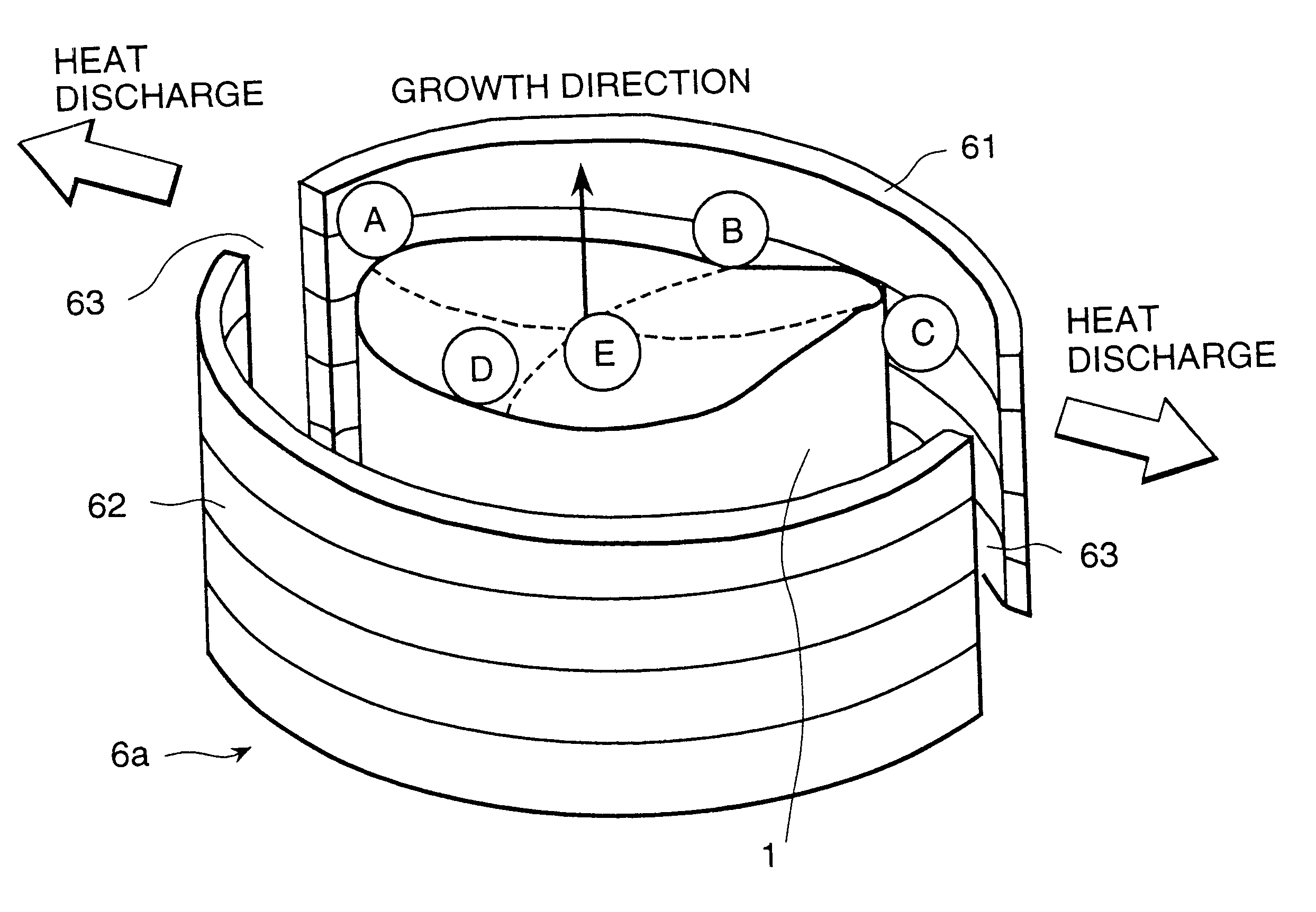
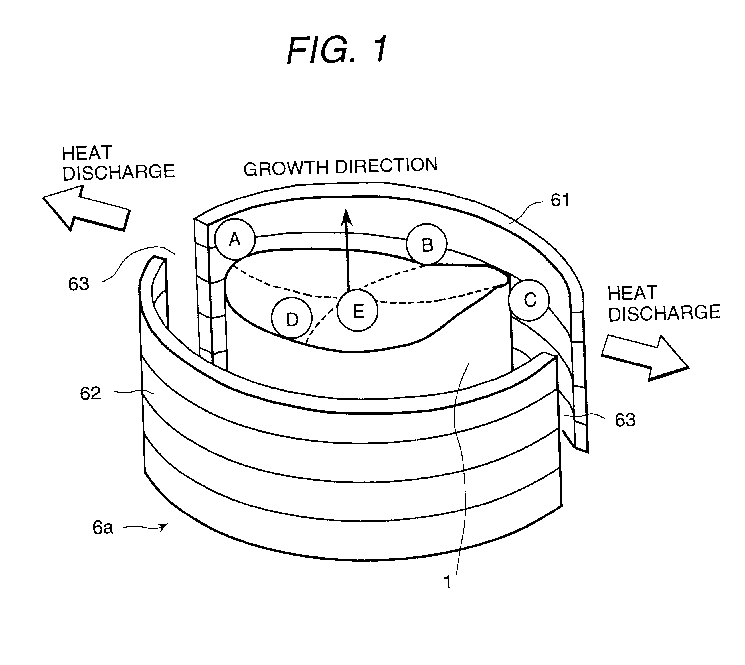
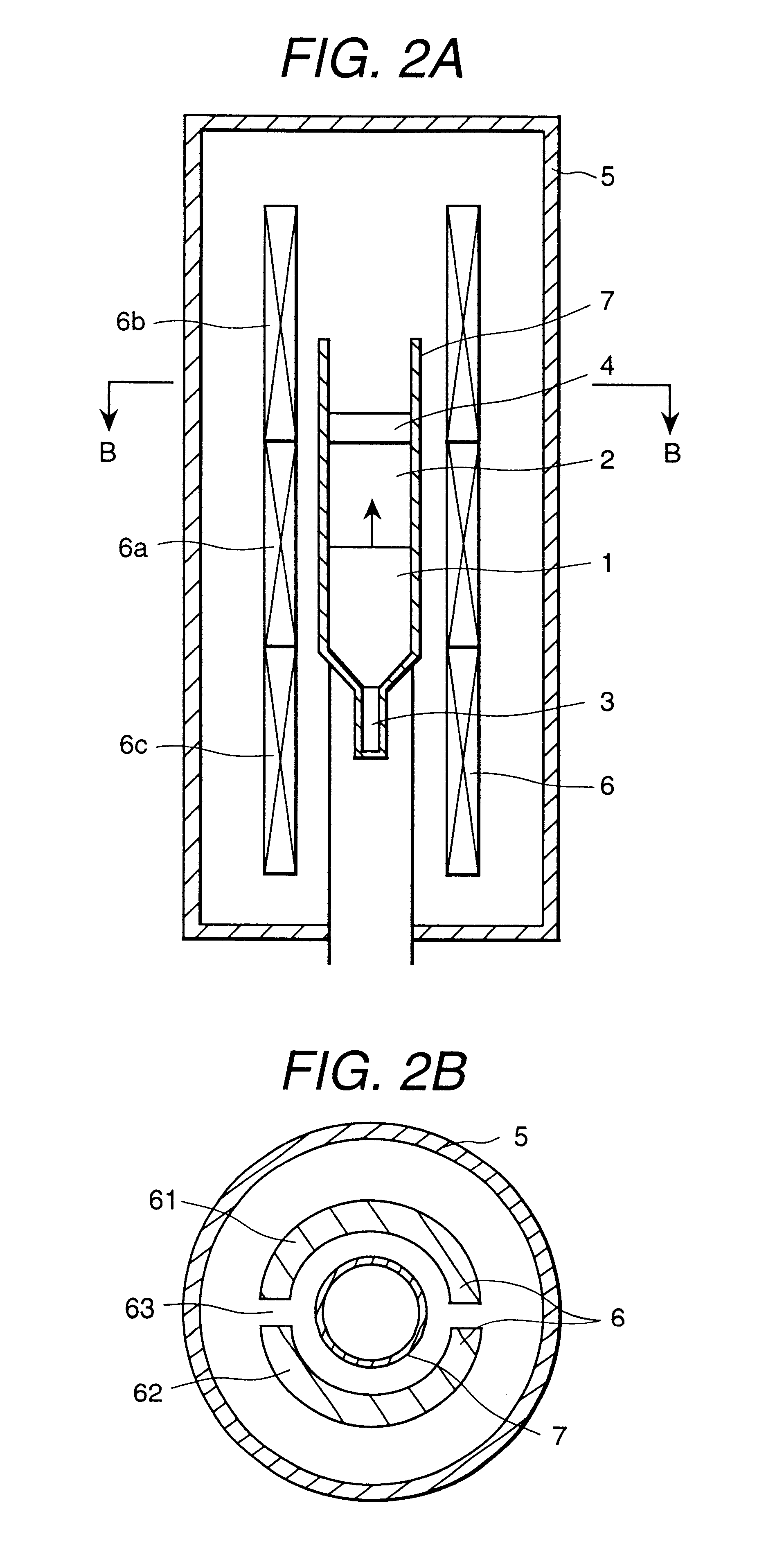
An embodiment will be described with reference to FIGS. 2A and 2B. The seed crystal 3, 3000 g of the GaAs material, a dopant Si and 200 g of B.sub.2 O.sub.3 4 were charged into a PBN crucible 7 having the inner diameter of .o slashed.80 mm. The crucible 7 was set in the electrical furnace. The heater 6 has an inner diameter of .o slashed.120 mm and is divided into halves. The width of the gap 63 where there is no heater was approximately 20 mm.

After N.sub.2 gas substituted for the atmosphere gas in the chamber 5, the temperature was increased. The temperature gradient was adjusted to 4.degree. C. / cm, the material was melted, and the seed was dipped into the melt. After that, the temperature was decreased at 1.degree. C. / h to grow a crystal. After completion of the growth, the crystal was cooled to the room temperature at 25 to 100.degree. C. / h and then taken out.

As a result of similarly carrying out the growing operation ten times, the yield of single crystal growth reached 90%. Whe...


PUM

PropertyMeasurementUnit
pressureaaaaaaaaaa
diameteraaaaaaaaaa
widthaaaaaaaaaa

Abstract

This invention relates to fabrication of a single crystal of a compound semiconductor according to the vertical Bridgman method which improves a recess in the interface between solid and melt and can obtain a stable yield of single crystal growth characterized in that a part for discharging the heat of a crucible to the outside in the radial direction is formed at least in a part in the circumferential direction of a heater part for controlling the interface between solid and melt in a heater which surrounds the crucible and a semiconductor melt is gradually solidified from a lower part to an upper part in the crucible while maintaining the interface between solid and melt in a saddle shape, thereby growing a single crystal.

Description

BACKGROUND OF THE INVENTION1. Field of the InventionThe present invention relates to method and apparatus for fabricating a single crystal of a compound semiconductor according to the vertical Bridgman method of growing a single crystal by gradually solidifying a semiconductor melt from a lower part to an upper part in a crucible.2. Description of Related ArtIn recent years, attention is being paid to the vertical Bridgman method as a method of obtaining a large GaAs crystal having the diameter exceeding 3 inches and a low dislocation density. According to the vertical Bridgman method, a crucible for containing a material and a seed crystal (seed) is placed on the inside of a heater of a vertical electric furnace and the material in the upper part is melt. After that, the seed is dipped into the melt and a single crystal is grown in the crucible from a lower part to an upper part, that is, from a lower part on the seed crystal side to an upper part.The method of growing a crystal by...

Claims


Application Information

Patent Timeline
Patent Type & Authority Patents(United States)
IPC IPC(8): C30B11/00C30B29/42H01L21/208
CPCC30B11/00C30B11/003C30B29/42Y10T117/1016Y10S117/90Y10T117/10
Inventor MIZUNIWA, SEIJIITANI, KENYAWACHI, MICHINORI
Owner HITACHI CABLE
Why Eureka
Try Eureka