Color cathode field emission device, cold cathode field emission display, and process for the production thereof

Inactive Publication Date: 2001-10-02
SONY CORP
View PDF12 Cites 24 Cited by
  • Summary
  • Abstract
  • Description
  • Claims
  • Application Information

AI Technical Summary

Benefits of technology

It is therefore an object of the present invention to provide a process for the production of cold cathode field emission devices, which can overcome the problems in the production of conventional Spindt type cold cathode field emission devices and which enables the production

Problems solved by technology

However, it is very difficult to vertically deposit the metal layer 101 having a uniform thickness all over the entire surface of a large-area dielectric supporting substrate for producing a large-area field emission display, and not only an in-plane variation of thickness of the metal layer 101 on the dielectric supporting substrate but also a variation of thickness among lots are also liable to occur.
Moreover, a large-scale deposition apparatus is required.
However, it is difficult to accurately form the above peeling-off layer 100 all over the entire surface of the dielectric supporting substrate having a large area, and it is also difficult to accurately deposit the peeling-off layer 100 such that the peeling-off layer 100 extends from the edge portion 15A of the opening portion 15 formed in the gate electrode 14 so as to have "eaves".
Furthermore, not only it is very

Method used


Image

  • Color cathode field emission device, cold cathode field emission display, and process for the production thereof
  • Color cathode field emission device, cold cathode field emission display, and process for the production thereof
  • Color cathode field emission device, cold cathode field emission display, and process for the production thereof

Examples


example 1

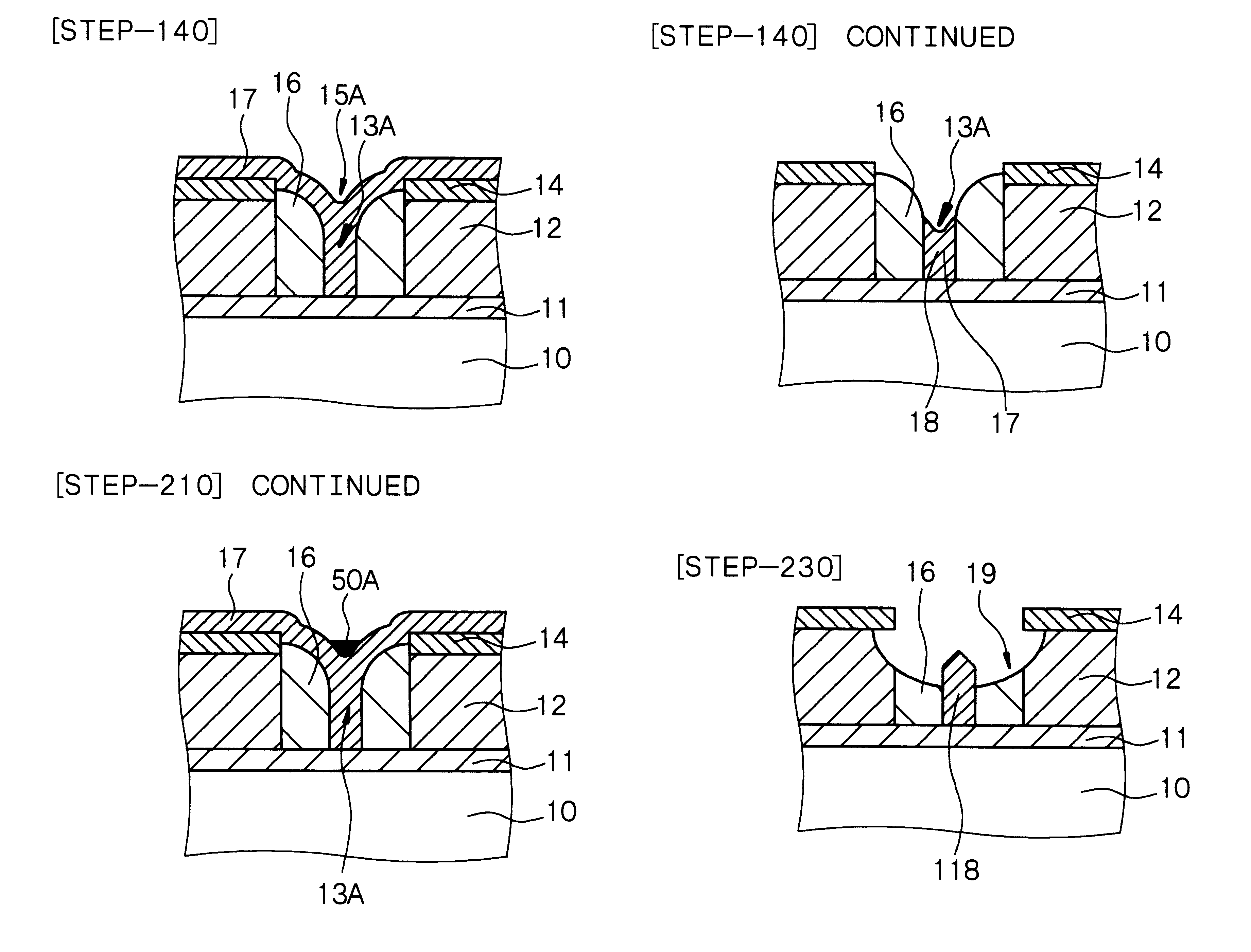
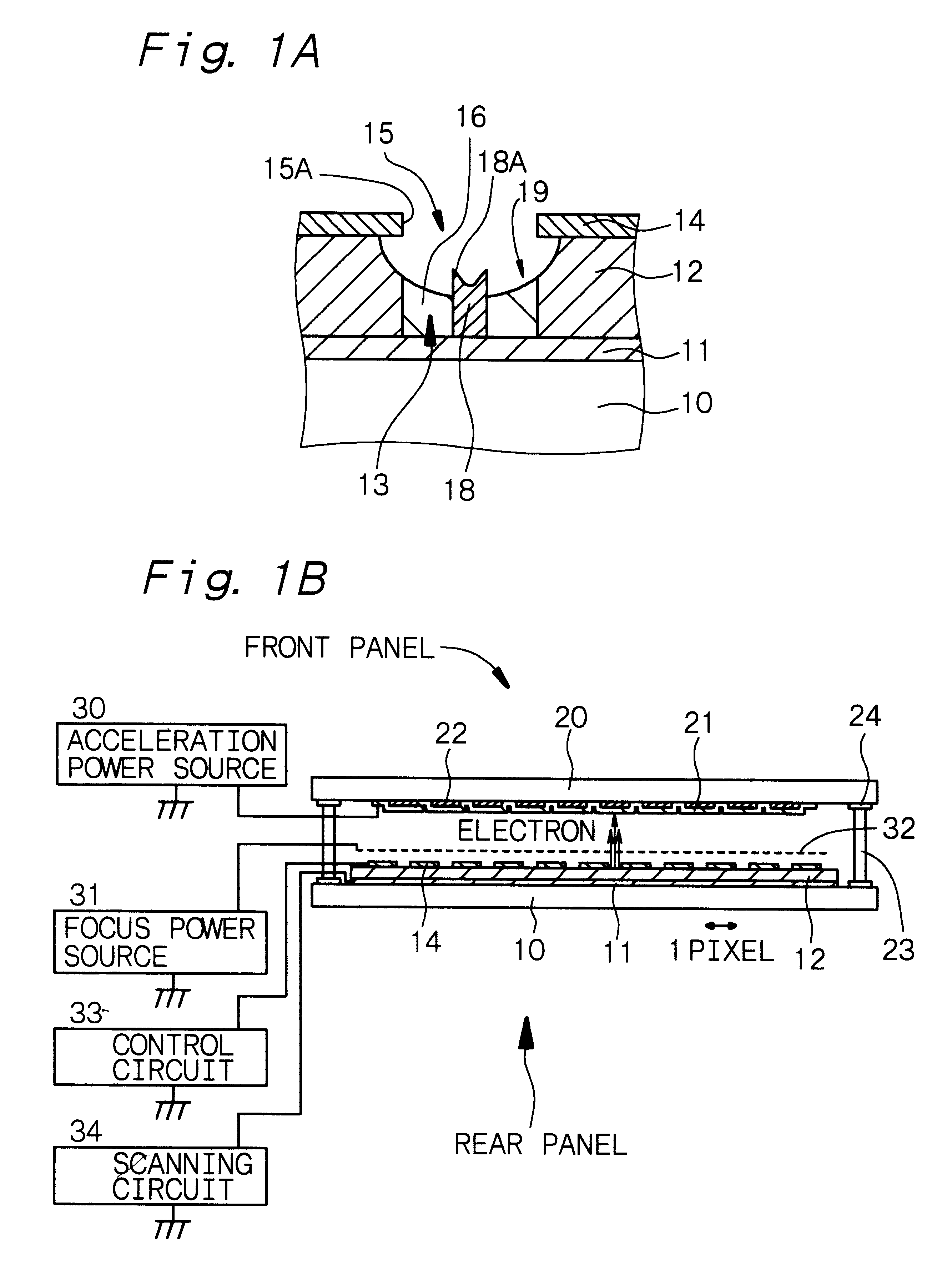
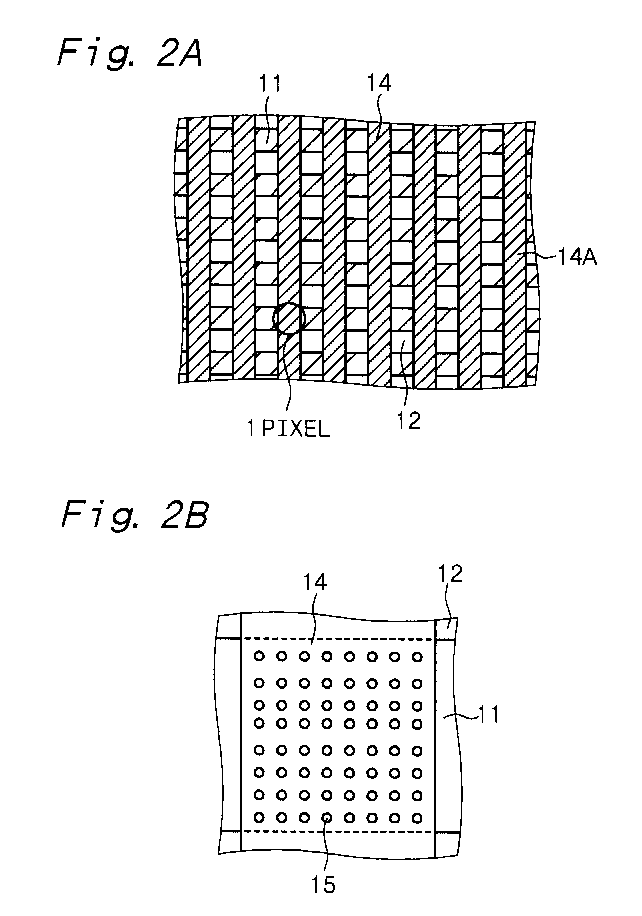
is concerned with a cold cathode field emission device (to be simply referred to as "field emission device" hereinafter), a cold cathode field emission display (to be simply referred to as "field emission display" hereinafter) having the field emission devices, and processes for the production thereof, according to the first aspect of the present invention. FIG. 1A shows a schematic partial end view of the field emission device in Example 1, and FIG. 1B shows a conceptual view of the field emission display when the field emission display is cut with a vertical plane. FIG. 2A shows a configuration of part of electrode layers (cathode electrode layers) 11 and gate electrodes 14 in the field emission display, FIG. 2B shows a configuration of the electrode layer (cathode electrode layer) 11 and the gate electrode 14 in one pixel, and FIG. 3A shows a schematic perspective view of the field emission display. In FIG. 2B, the number of the field emission devices constituting one pixel is 64...

example 2

Example 2 is a variant of Example 1. The field emission device of Example 2 differs from the counterpart of Example 1 in the form of top surface of the field emission device. That is, in Example 2, as shown in FIG. 8A, an acute-angled portion 18G is formed on a top surface 18F of an emitter electrode 118, and the acute-angled portion 18G is constituted of a tip end surface 18H projecting toward the central portion of the top surface. That is, the top surface 18F of the emitter electrode 118 has a conical form. The emitter electrode 118 in Example 2 is formed, after a gate electrode 14 is formed on an insulating interlayer 12, by forming opening portions 15 and 13 which penetrate the gate electrode 14 and the insulating interlayer 12 and have a bottom portion where an electrode layer (cathode electrode layer) 11 is exposed; forming a side-wall 16 composed of an insulating material on the side walls of the opening portion 13 and 15, to decrease the opening portions 13 and 15 in diamet...

example 3

Example 3 is concerned with the field emission device, the field emission display and the processes for the production thereof, according to the second aspect of the present invention. FIG. 10A shows a schematic partial end view of the field emission device of Example 3. When cut with a perpendicular plane, the field emission display of Example 3 has a conceptual view similar to that shown in FIG. 1B. Further, for a configuration of part of the electrode layers (cathode electrode layers) 11 and the gate electrodes 14 in the field emission display, a configuration of the electrode layer (cathode electrode layer) 11 and the gate electrode 14 in one pixel and a perspective view of the field emission display, see FIGS. 2A, 2B and 3A. Further, the basic configuration of the field emission device in Example 3 is similar to the configuration of the field emission device explained in Example 1, and the emitter electrode 18 has a top portion as shown in the enlarged view of FIG. 3B.

The emitt...


PUM


Abstract

A process for the production of a cold cathode field emission device comprising the steps of; (A) forming a patterned electrode layer on a dielectric supporting substrate, (B) forming an insulating interlayer on the dielectric supporting substrate and the electrode layer, (C) forming a gate electrode constituted of a first conductive layer on the insulating interlayer, (D) forming an opening portion which penetrates through at least the insulating interlayer and has a bottom portion where the electrode layer is exposed, (E) forming a side-wall of an insulating material on the side wall of the opening portion, to decrease the opening portion in diameter, (F) forming a second conductive layer on the entire surface including the inside of the opening portion by a physical or chemical vapor deposition method, (G) etching back the second conductive layer to form an emitter electrode shaped in the form of a column and constituted of the second conductive layer in the opening portion, and (H) removing at least an upper portion of the side-wall.

Description

BACKGROUND OF THE INVENTION AND RELATED ART STATEMENTThe present invention relates to a cold cathode field emission device, a cold cathode field emission display and processes for the production thereof. More specifically, it relates to a cold cathode field emission device having the form of a column, a flat panel type cold cathode field emission display having a plurality of the cold cathode field emission devices arranged in a two-dimensional matrix, and processes for the production thereof.Studies are being made on various flat panel type displays for an image displaying unit which is to replace currently main-stream cathode ray tubes (CRT). The flat type displays include a liquid crystal display (LCD), an electroluminescence display (ELD) and a plasma display (PDP). Further, there is also proposed a cold cathode field emission display from the viewpoint of a brightness on displaying.The above cold cathode field emission display (to be sometimes simply referred to as "field emiss...

Claims


Application Information

Patent Timeline
IPC IPC(8): H01J1/304H01J9/02H01J1/30
CPCH01J1/3042H01J9/025
Inventor KIKUCHI, KAZUOKUBOTA, SHINJI
Owner SONY CORP
Why Eureka
Try Eureka