Semiconductor device having an internal voltage generating circuit

a technology of internal voltage generation and semiconductors, applied in the direction of digital storage, process and machine control, instruments, etc., can solve the problems of low efficiency of circuits in operation, inability to reduce the occupied area, and low miniaturization of processors and logics

Inactive Publication Date: 2001-10-02
MITSUBISHI ELECTRIC CORP
View PDF5 Cites 110 Cited by
  • Summary
  • Abstract
  • Description
  • Claims
  • Application Information

AI Technical Summary

Problems solved by technology

However, external devices such as a processor and a logic have not been highly miniaturized compared with the semiconductor memory devices, and therefore relatively high operation power supply voltages are used for maintaining intended operation speeds.
Meanwhile, the peripheral circuits in operation consume a current smaller than that in the operation of the sense amplifier.
This results in a problem that the reference voltage generating circuits occupy a large area in internal power supply circuit 500, and the occupied area cannot be reduced.
Due to provision of independent reference voltage generating circuits 502s and 502p, trimming of the voltage levels of reference voltages Vrefs and Vrefp must be performed independently of each other, and the voltage trimming requires a long time.
Thus, the voltage level of internal power supply voltage Vcc is stabilized after the voltage level of reference voltage Vref is stabilized, and therefore it is impossible to rapidly stabilize internal power supply voltage Vcc after starting of supply of external power supply voltage Vext.
Therefore, an unnecessarily high voltage is applied to internal power supply line 505d due to, e.g., noises, which may result in instantaneous breakdown, i.e., breakdown of circuits utilizing internal power supply voltage Vcc on internal power supply line 505d and/or degradation of the reliability thereof (due to application of large voltage stresses upon each power-on).
For rapidly stabilizing internal power supply voltage Vcc, complicated adjustment of timing of power-on detection signal /POR is required, and therefore it is difficult to ensure a reliability of the internal circuits.
Further, if power-on detection signal /POR is held in the active state at L-level for a long period as shown by broken line in FIG. 51, internal power supply voltage Vcc is dr...

Method used


Image

  • Semiconductor device having an internal voltage generating circuit
  • Semiconductor device having an internal voltage generating circuit
  • Semiconductor device having an internal voltage generating circuit

Examples


embodiment 1

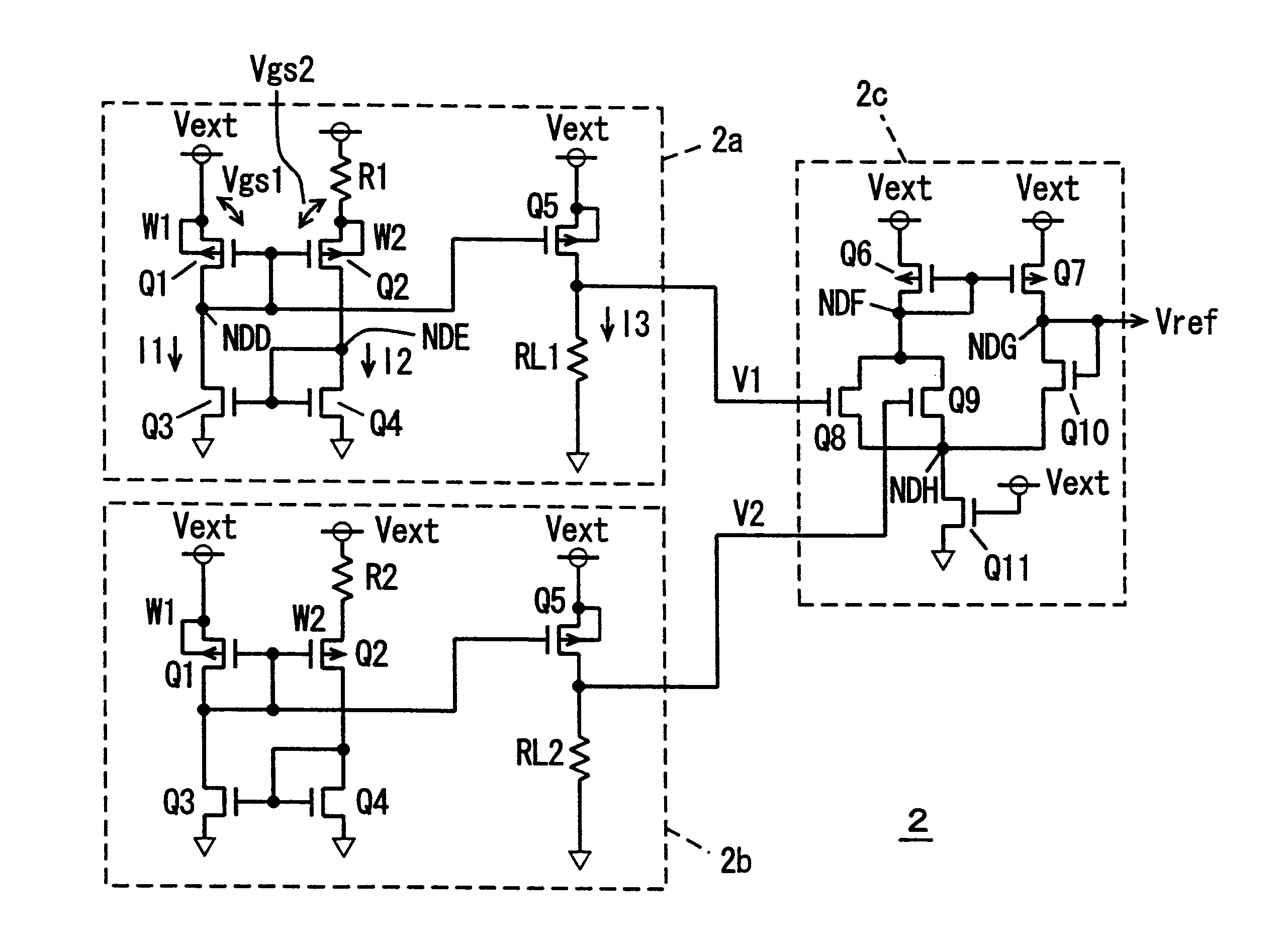
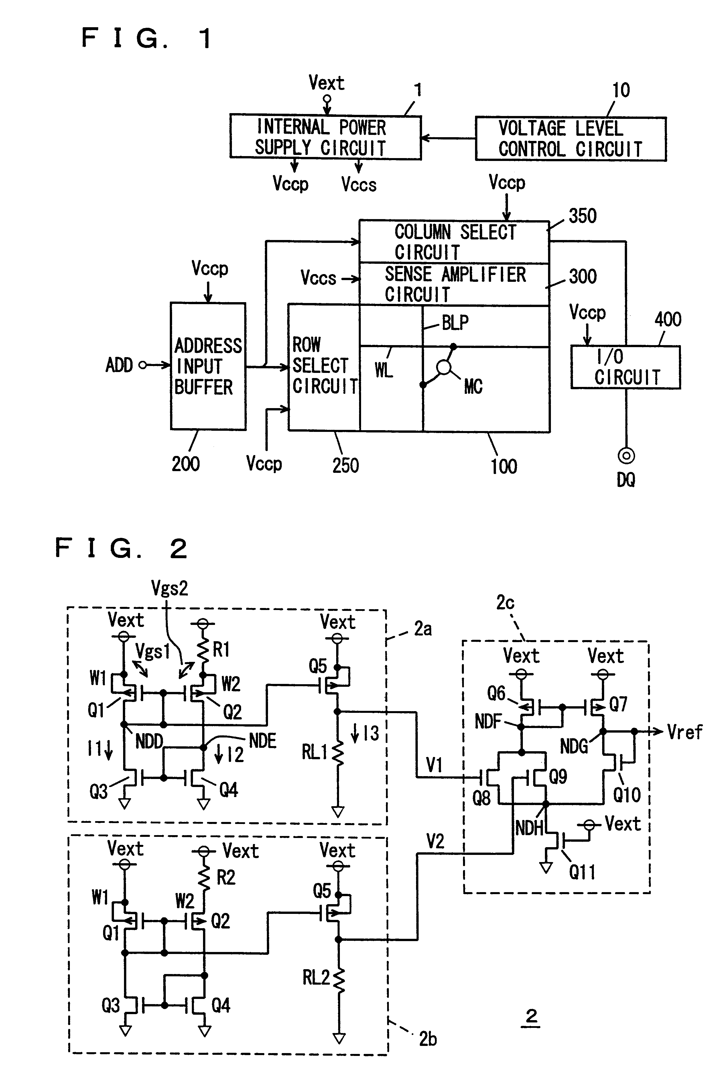
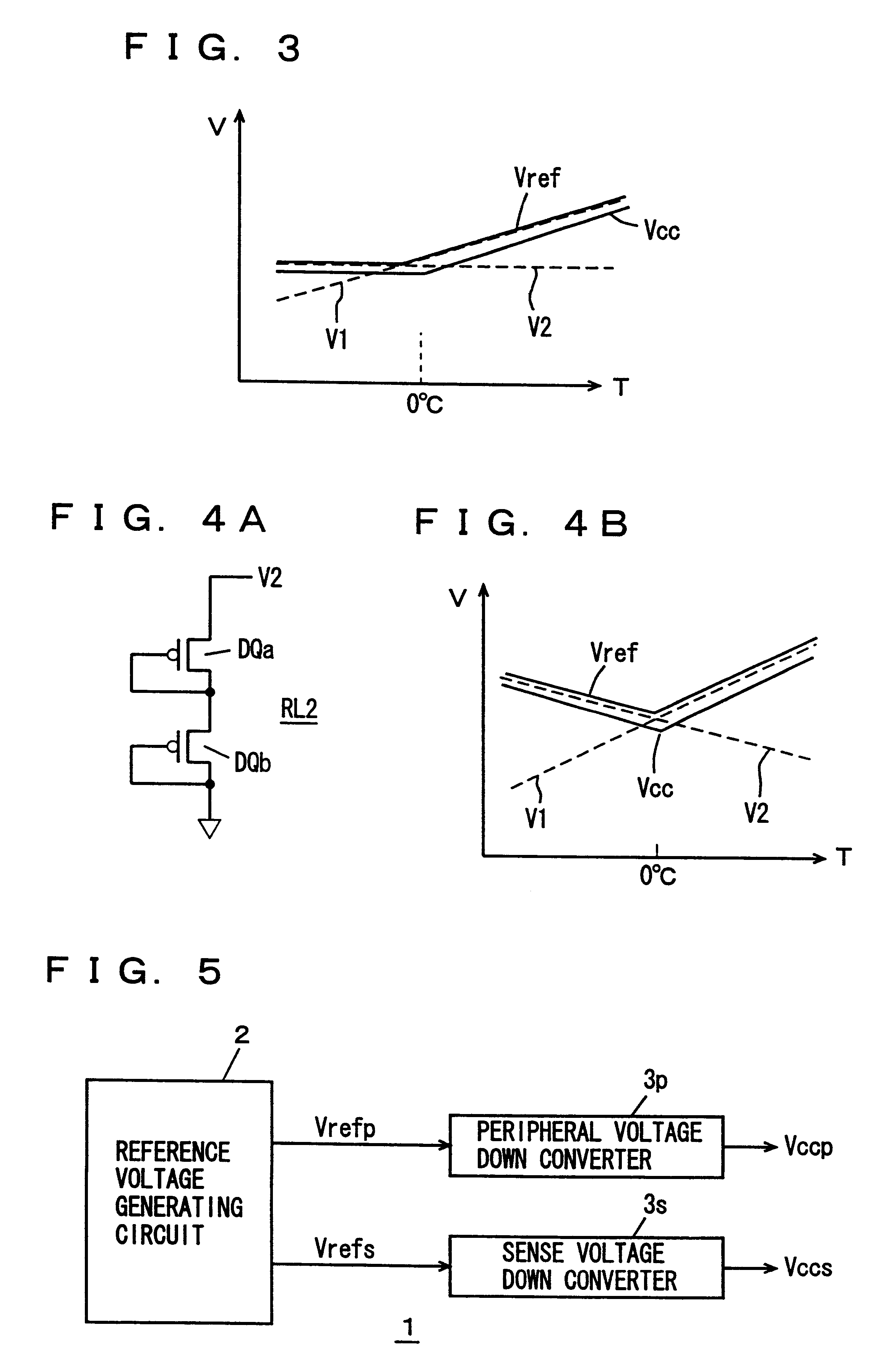
FIG. 2 shows a structure of the reference voltage generating circuit according to the invention. In FIG. 2, reference voltage generating circuit 2 includes a first voltage generating circuit 2a generating a first voltage V1 having a positive temperature characteristic that the voltage level thereof rises with increasing of temperature, a second voltage generating circuit 2b generating a second voltage V2 having a negative of zero temperature characteristic that the voltage level lowers or is kept constant with increasing of temperature, and an OR circuit 2c for selecting a voltage at a higher voltage level between first and second voltages V1 and V2, for generation as reference voltage Vref.

First voltage generating circuit 2a includes a p channel MOS transistor Q1 which is connected between an external power supply node and a node NDD and has a gate connected to node NDD, a p channel MOS transistor Q2 which has a source connected to an external power supply node via a resistance ele...

embodiment 2

FIG. 5 shows a structure of a main portion of a semiconductor memory device according to an embodiment 2 of the invention. FIG. 5 schematically shows a structure of the internal power supply circuit 1 shown in FIG. 1. In internal power supply circuit 1 shown in FIG. 5, a peripheral voltage down converter 3p producing peripheral power supply voltage Vccp and a sense voltage down converter 3s producing sense power supply voltage Vccs are supplied with peripheral reference voltages (i.e., reference voltage for peripheral circuits) Vrefp and Vrefs commonly from reference voltage generating circuit 2. Since single reference voltage generating circuit 2 is used for producing peripheral reference voltage Vrefp and sense reference voltage Vrefs, a circuit occupation area and a current consumption can be reduced. Further, reference voltages Vrefp and Vrefs can have the same temperature characteristics, and the temperature characteristics and voltage levels of internal power supply voltages V...

embodiment 3

FIG. 12 schematically shows a structure of a main portion of a semiconductor memory device according to an embodiment 3 of the invention. FIG. 12 shows the structure of a sense power supply circuit for transmitting sense power supply voltage Vccs to a sense amplifier circuit 300. In FIG. 12, the sense power supply circuit includes a sense reference voltage generating circuit 2s generating sense reference voltage Vrefs, a peripheral reference voltage generating circuit 2p generating peripheral reference voltage Vrefp, a select circuit 4 for selecting one of reference voltages Vrefs and Vrefp in response to a switch signal .phi.SW, and a sense voltage down converter 3s performing a voltage down-converting operation to produce sense power supply voltage Vccs in accordance with the selected reference voltage from select circuit 4. Sense reference voltage generating circuit 2s and peripheral reference voltage generating circuit 2p may be independent of each other, or may be provided in a...


PUM


Abstract

An internal power supply circuit produces an internal power supply voltage from an external power supply voltage. A voltage level control circuit controls a voltage level and a temperature characteristic of the internal power supply voltage generated by the internal power supply circuit. The internal power supply circuit produces the internal power supply voltage having a negative or zero temperature characteristic in a low temperature region and a positive temperature characteristic in a high temperature region. The voltage level control circuit includes a structure optimizing a capacitance value of a sense power supply line stabilizing capacitance for driving a sense amplifier circuit, a level converting circuit determining the lowest operable region of the external power supply voltage of the internal power supply circuit, or a structure forcedly operating the internal voltage down converter upon power-on. The internal power supply voltage at a desired level is stably produced with a small occupied area and a low current consumption.

Description

1. Field of the InventionThe present invention relates to a semiconductor device, and particularly to a structure of an internal voltage generating circuit for internally generating a voltage at a desired level.2. Description of the Background ArtFIG. 47 schematically shows a whole structure of a conventional semiconductor memory device. In FIG. 47, the semiconductor memory device includes a memory cell array 100 having a plurality of memory cells MC arranged in rows and columns. In memory cell array 100, word lines WL are arranged corresponding to the rows of memory cells MC, respectively, and bit line pairs BLP are arranged corresponding to the columns of memory cells MC, respectively. Memory cells MC are arranged corresponding to crossings between bit line pairs BLP and word lines WL, respectively.The semiconductor memory device further includes an address input buffer 200 which takes in an externally supplied address signal ADD to produce an internal address signal, a row select...

Claims


Application Information

Patent Timeline
IPC IPC(8): G05F1/46G05F1/10G11C11/413G05F3/24G05F3/26G11C5/14G11C11/401G11C11/407G11C11/409
CPCG05F1/465
Inventor MITSUI, KATSUYOSHIFURUTANI, KIYOHIROKONO, TAKASHI
Owner MITSUBISHI ELECTRIC CORP
Why Eureka
Try Eureka