Optical waveguide circuit, its manufacturing method and optical waveguide module having the optical waveguide circuit

a manufacturing method and optical waveguide technology, applied in the field of optical waveguide circuits, its manufacturing methods and optical waveguide modules having optical waveguide circuits, can solve the problems of unnecessary temperature control, increase the volume and price of the entire lightwaveguide grating multiplexer, and complicate the structur

Inactive Publication Date: 2001-10-16
NIPPON TELEGRAPH & TELEPHONE CORP +1
View PDF3 Cites 85 Cited by
  • Summary
  • Abstract
  • Description
  • Claims
  • Application Information

AI Technical Summary

Benefits of technology

To achieve the above object, according to a conception 1 of the present invention there is provided, in a lightwaveguide circuit including a plurality of waveguides of different optical path lengths, wherein, a core and an upper clad, a material having a temperature coefficient including a refractive index including a symbol different from that of a temperature coefficient of an effective refractive index of the waveguide is ("temperature compensating material" hereinafter) charged into at least one of a groove formed by removing an upper clad and a core from the waveguide, and a groove formed by removing the upper clad, the core and the lower clad from the waveguide, and a difference in length of the removed portions between adjacent waveguides is proportional to a difference in length of the waveguides which was not removed and remained.

Problems solved by technology

Further, a power source, control apparatus or the like is required for operating the Peltier element or heater, which increase a volume and price of the entire lightwaveguide grating multiplexer.
For this reason, it had been required to remove the temperature dependency of the lightwaveguide circuit itself, and to unnecessitate the temperature control.
However, in this method, two kinds of cores having different materials are intermingled on the same substrate, which complicates the structure and thus, it is not manufactured easily.
Therefore, if the temperature is changed, a difference of refractive index of the core and the clad is changed, and if worst comes worst, the waveguide may not introduce light and therefore, this method can not keep up with wide change of environment temperature.

Method used


Image

  • Optical waveguide circuit, its manufacturing method and optical waveguide module having the optical waveguide circuit
  • Optical waveguide circuit, its manufacturing method and optical waveguide module having the optical waveguide circuit
  • Optical waveguide circuit, its manufacturing method and optical waveguide module having the optical waveguide circuit

Examples


first embodiment

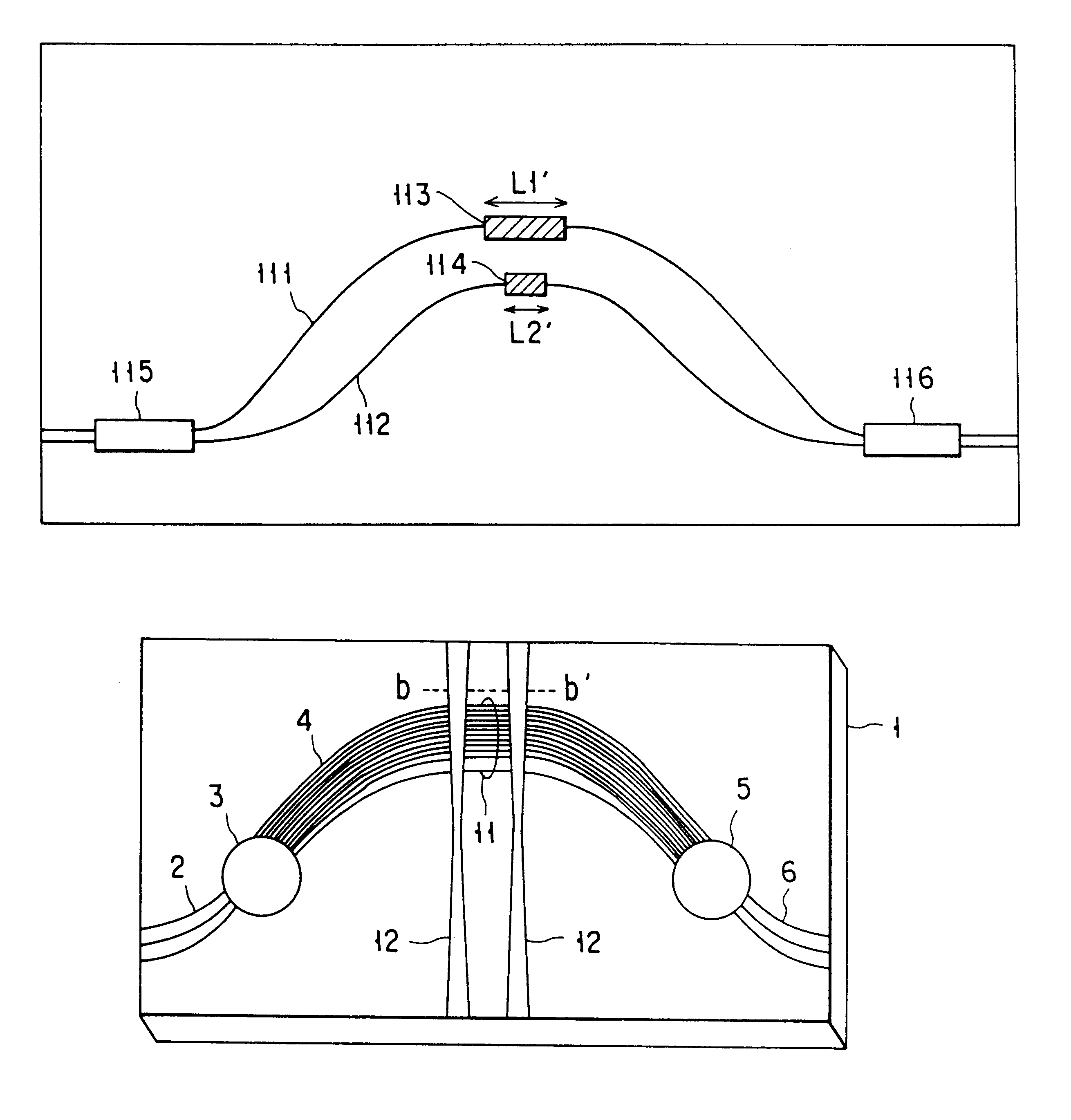
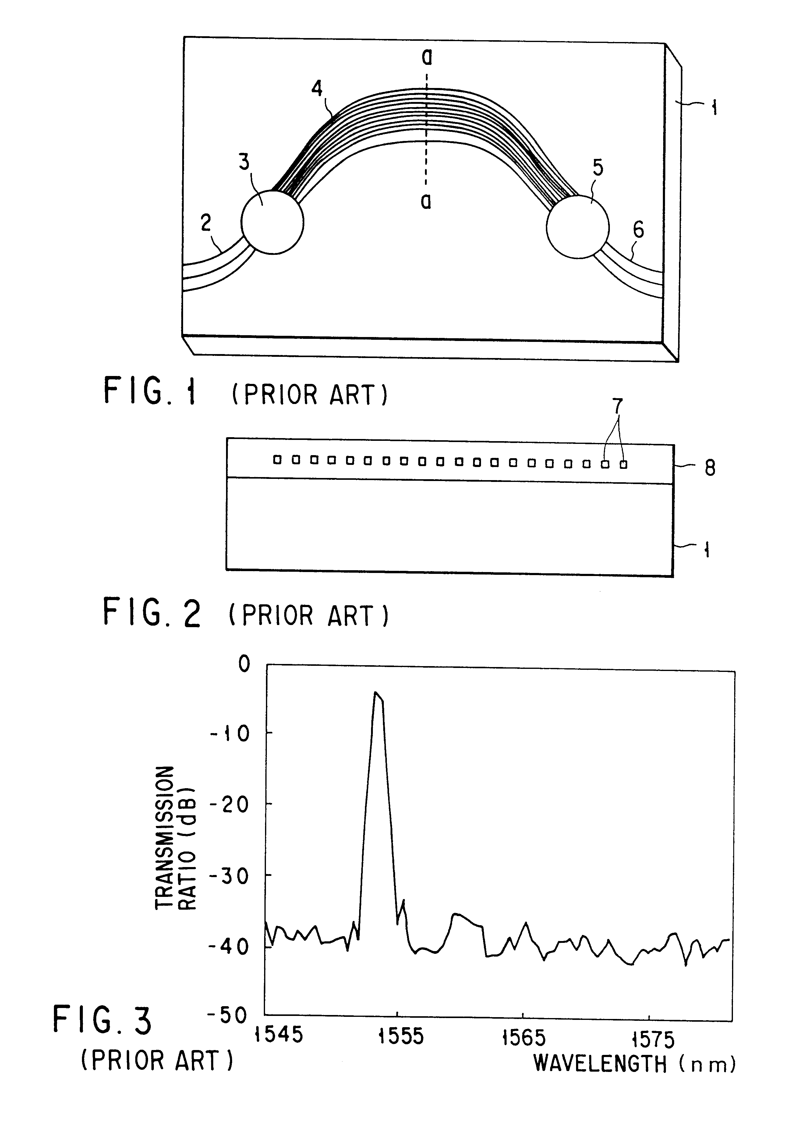
FIG. 8 shows a temperature independent arrayed-waveguide grating multiplexer according to a first embodiment of the present invention, and FIG. 9 shows an enlarged sectional view taken along the line b-b' in FIG. 8. An arrayed-waveguide 4 shown in FIG. 8 of the conventional arrayed-waveguide grating multiplexer (FIG. 1) is provided at its central portion with a straight waveguide portion 11 for forming a groove. Si substrate 1, input waveguide 2, a first slab waveguide 3, a second slab waveguide 5, output waveguide 6 and a groove 12 are provided.

A method for producing the waveguide of the invention will be described with reference to FIG. 10.

Step Q1: A quartz glass is accumulated on the Si substrate 1 in an amount of 30 .mu.m by flame-accumulating process, and is transparentized in an electric furnace.

Step Q2: Then, a core glass in which Ge is added is accumulated on the glass film which is accumulated in step Q1 in an amount of 7 .mu.m by flame-accumulating process, and is transpar...

second embodiment

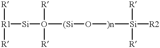
A second embodiment is the same as the first embodiment except that a gelled polymethyl phenyl siloxane was used as a temperature compensating material. In the present embodiment, vinyl terminal polymethyl phenyl siloxane, methyl hydride siloxane and platinum catalyst were charged into the groove and reacted for 30 minutes at 150.degree. C., thereby preparing a temperature compensating material. Substantially the same effect as the first embodiment was confirmed.

third embodiment

FIG. 13 shows a temperature independent arrayed-waveguide grating multiplexer according to a third embodiment, and FIG. 14 shows an enlarged sectional view taken along the line c-c' in FIG. 13. The third embodiment differs from the first embodiment in that a plurality of narrow grooves are formed by photolithography and reactive ion etching. As shown in FIG. 15, a radiation loss is abruptly increased with respect to a width of the groove of the present invention, i.e., a length of the cut waveguide. Therefore, a radiation loss when ten grooves of 10 .mu.m width are formed is smaller than a radiation loss when a single groove of 100 .mu.m width is formed.

Thereupon, taking reproduction performance of etching into account, the minimum groove width was set to be 10 .mu.m, and the number of grooves was set five. A length of the cut waveguide is increased by 0.25 .mu.m each. At that time, a radiation loss was 1 dB. As compared with the first embodiment, the radiation loss is reduced down ...


PUM


Abstract

In a light waveguide circuit including a plurality of waveguides having different length, a material (10) having a temperature coefficient of a refractive index including a symbol different from that of a temperature coefficient of an effective refractive index of the waveguide (4) is charged into a groove (12) formed by removing the upper clad and the core from the waveguide (4), or a groove (12) formed by removing the upper clad, the core and the lower clad from the waveguide (4). A difference in length of the removed portions between adjacent waveguides is proportional to a difference in length of the waveguides which were not removed and remained.

Description

This application is the national phase of international application PCT / JP98 / 00626 filed Feb. 16, 1998 which designated the U.S.1. Technical FieldThe present invention relates to a light waveguide circuit used in a field of an optical communication or an optical information processing, a producing method thereof and a light waveguide circuit module having such a lightwaveguide circuit, and more particularly, to a waveguide type optical element whose optical characteristic does not depend on a temperature, and more specifically, a lightwaveguide circuit such as a lightwavelength grating multiplexer constituted by a waveguide formed on a planar substrate and optical characteristic thereof does not depend on a temperature.2. Background ArtRecently, studies and developments have actively been made for planar lightwave circuits (PLC) comprising quartz glass lightwaveguide formed on a silicone substrate.In such a planar lightwave circuit, a lightwavelength grating multiplexing function is...

Claims


Application Information

Patent Timeline
Patent Type & Authority Patents(United States)
IPC IPC(8): G02B6/34
CPCG02B6/12011G02B6/12014G02B6/12023G02B6/12028G02B6/42
Inventor INOUE, YASUYUKIKANEKO, AKIMASATAKAHASHI, HIROSHIHANAWA, FUMIAKIHATTORI, KUNINORIYOKOYAMA, KENJISUZUKI, SENICHISUMIDA, SHINOKAMOTO, KATSUNARIISHII, MOTOHAYAYAMADA, HIROAKIYOSHIDA, TAKASHIARISHIMA, KOICHIEBISAWA, FUMIHIRONAKAHARA, MOTOHIRO
Owner NIPPON TELEGRAPH & TELEPHONE CORP
Why Eureka
Try Eureka