Method for trimming the temperature coefficient of a floating gate voltage reference

a voltage reference and temperature coefficient technology, applied in static storage, digital storage, instruments, etc., can solve the problems of difficult reference tuning, long silicon iterations, and large amount of silicon, and achieve precise and stable reference voltage, good precision, and good precision

Active Publication Date: 2008-01-29
SEMICON COMPONENTS IND LLC
View PDF10 Cites 53 Cited by
  • Summary
  • Abstract
  • Description
  • Claims
  • Application Information

AI Technical Summary

Benefits of technology

[0013]The voltage reference circuit is then configured to perform a read operation, by coupling the first NVM transistor in a current mirror configuration with the reference NVM transistor. During the read operation, the control gates of the first and reference NVM transistors are coupled to receive the ground supply voltage, and the drains of the first and reference NVM transistors are coupled to input terminals of a differential amplifier. The output terminal of the differential amplifier is coupled to the floating gate of the reference NVM transistor through the first set of capacitors (while the second set of capacitors remains connected between the floating gate and control gate of the reference NVM transistor). Under these conditions, the differential amplifier provides a single-ended output voltage that is precisely equal to the programmed threshold voltage of the first NVM transistor. In accordance with one embodiment of the present invention, the output voltage can be adjusted by shifting capacitors between the first and second sets of capacitors. In one embodiment, the capacitors available for shifting have a binary weighting, thereby enabling precise control of the output voltage.
[0014]In accordance with one embodiment, the first and reference NVM transistors are matched. In addition, the MOS transistors used to couple these NVM transistors in the various current mirror configurations are matched. Using matched MOS devices cancels the first order variations of the programmed reference voltage as compared to the desired value. By using the reference NVM transistor and associated MOS devices as a reference in the differential programming circuit, even second order voltage shifts are canceled, thus realizing a very precise and stable reference voltage. In one embodiment, the programming operations are automatically stopped with the floating gate voltages at the desired values by implementing a quasi-read function during the programming steps. Because the programming does not affect the mirror matching, the programmed reference has very good precision and very low intrinsic temperature coefficient.

Problems solved by technology

There are significant drawbacks with this classical approach, including: (1) the reference tuning is difficult and requires lengthy silicon iterations, (2) the operation at low currents requires very large resistors, and (3) the overall circuit is rather complicated and expensive in terms of silicon area.
Moreover, the classical band-gap circuits have difficulty achieving a very low temperature coefficient due to inherent second order temperature effects.
Trimming the reference to values other than the silicon band-gap requires additional circuits and involves a significant increase in area consumption.
For the same reason, such floating nodes cannot be used as direct reference voltages, since they cannot drive any current.
The use of a single floating node of a non-volatile memory cell to generate a voltage reference has a number of drawbacks, including: (1) the circuit required to program the single floating node introduces a capacitive coupling, which produces an offset between the programmed voltage and the read voltage, (2) charge de-trapping occurring after the programming step introduces another uncertainty in the final programmed reference voltage, (3) programming stress can unpredictably change the characteristics of the non-volatile memory cell, such that resistor trimming is necessary, and (4) to obtain the lowest temperature coefficient, measurements at different ambient temperatures are required.
All these impose serious restrictions in the manufacturing process for voltage references using a single floating node of a non-volatile memory cell.
There are number of drawbacks associated with this type of non-volatile reference.
The use of hot electrons injection for charge injection makes the precise programming very difficult, because hot electron injection is very fast and non-linear with time.
As a result, the precise programming of a reference voltage is a difficult task.
Further complications arise from the fact that the differential reference voltage is obtained as voltage floating above the ground, so additional analog processing is needed to transfer the differential reference voltage to a single ended reference voltage.
The additional circuitry not only adds to the cost of the solution but also introduces distortions that diminish the accuracy of the reference voltage.

Method used


Image

  • Method for trimming the temperature coefficient of a floating gate voltage reference
  • Method for trimming the temperature coefficient of a floating gate voltage reference
  • Method for trimming the temperature coefficient of a floating gate voltage reference

Examples


Embodiment Construction

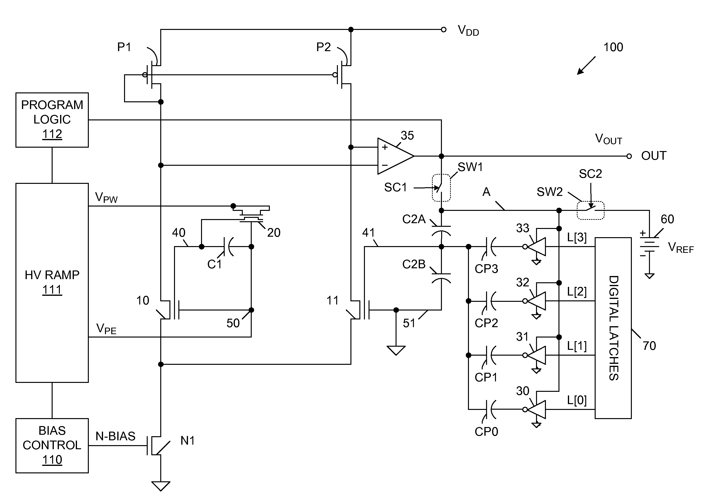
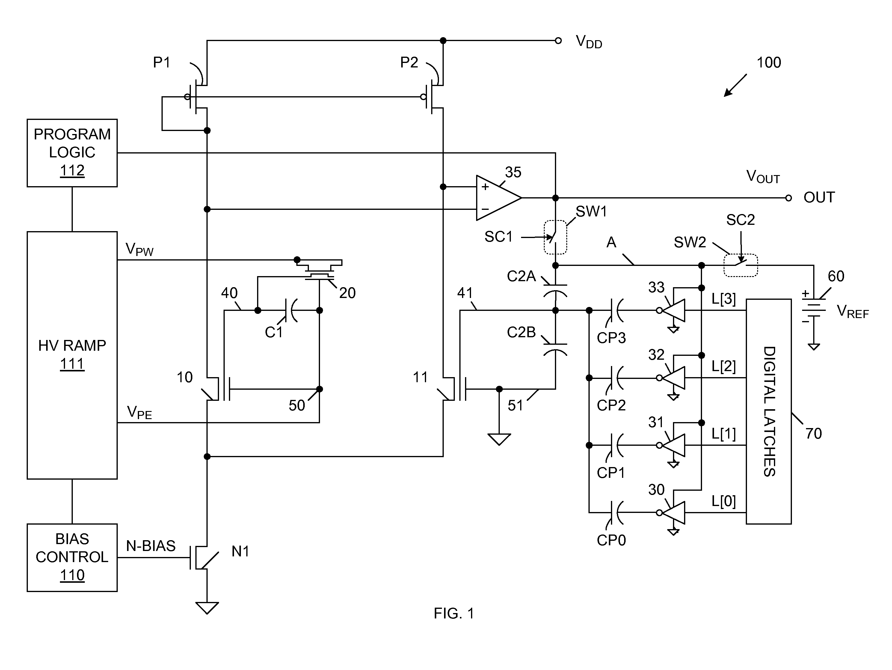
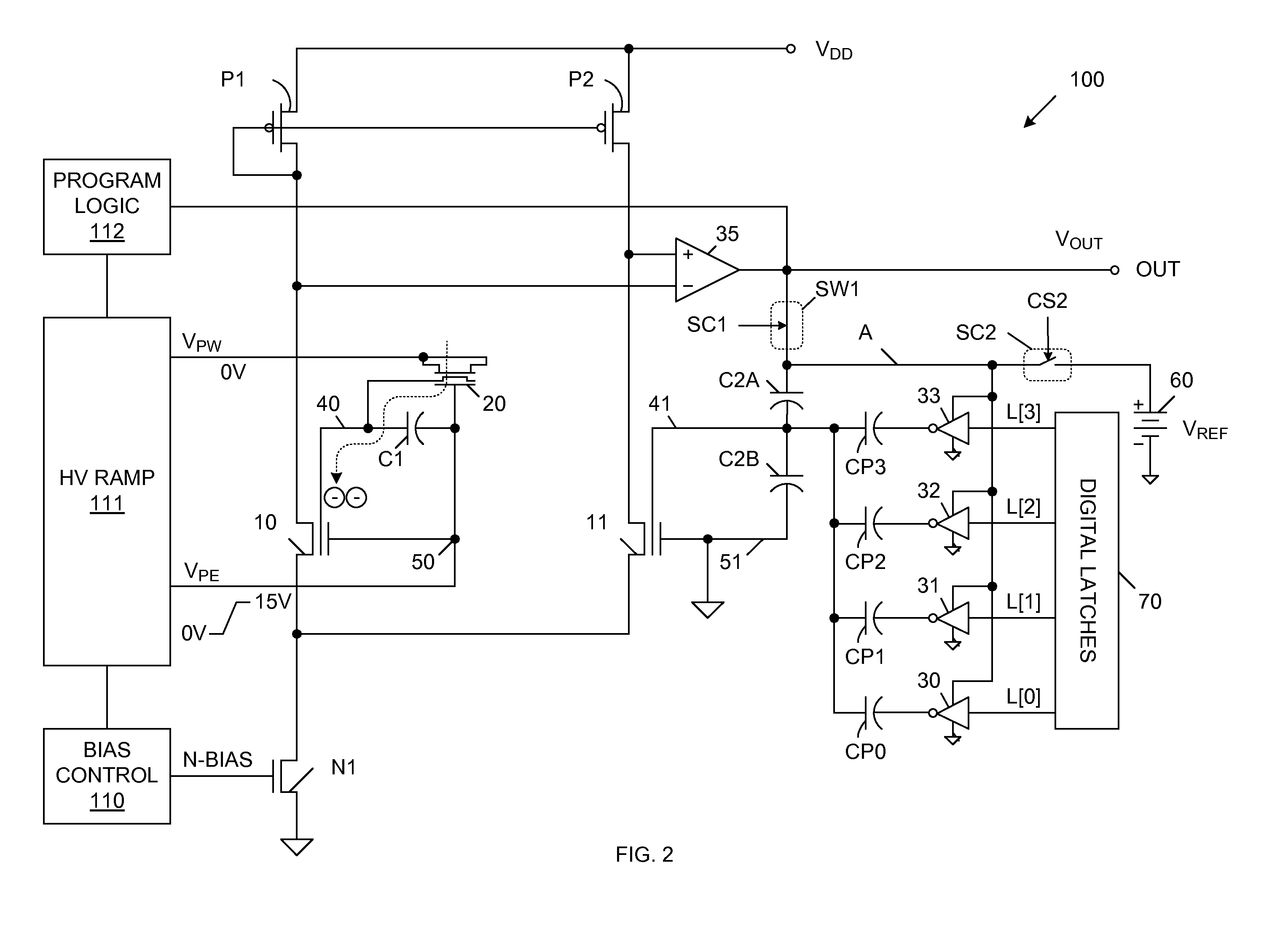
[0024]FIG. 1 is a circuit diagram of a CMOS voltage reference circuit 100 in accordance with one embodiment of the present invention. Voltage reference circuit 100 includes non-volatile memory (NVM) transistors 10-11, thin-dielectric tunnel capacitor 20, p-channel MOS transistors P1-P2, n-channel MOS transistor N1, capacitors C1, C2A, C2B, CP0, CP1, CP2 and CP3, inverter circuits 30-33, differential amplifier 35, switches SW1-SW2, reference voltage supply 60 and digital latches 70.

[0025]Non-volatile memory transistors 10-11 include floating gates 40-41, respectively, and control gates 50-51, respectively. Each of non-volatile memory transistors 10-11 has a standard double polysilicon gate structure with a dielectric thickness large enough (e.g., greater than 150 Angstroms) to prevent charge leakage from the floating gates 40-41. In one embodiment, each of the floating gates 40-41 is separated from the corresponding control gate 50-51 by a dielectric with effective silicon dioxide th...


PUM


Abstract

A voltage reference circuit provides a reference voltage that can be precisely programmed. The threshold voltage of a first non-volatile memory (NVM) transistor is programmed while coupled in parallel with a second NVM transistor. During programming, one or more capacitors are connected between the floating gate of the first NVM transistor and ground, and one or more capacitors are connected between the floating gate of the second NVM transistor and ground. The first and second NVM transistors are then coupled to a differential amplifier, which is used to generate a single-ended reference voltage in response to the programmed threshold voltage of the first NVM transistor. Bipolar transistors are selectively switched between the various capacitors and ground, thereby providing precise adjustment of the temperature coefficient of the voltage reference circuit.

Description

RELATED APPLICATIONS[0001]The present application is a continuation-in-part of U.S. patent application Ser. No. 11 / 355,394 filed Feb. 15, 2006 now U.S. Pat. No. 7,245,536.BACKGROUND OF THE INVENTION[0002]1. Technical Field[0003]The present invention is in the field of non-volatile programmable integrated circuits.[0004]2. Description of Related Art[0005]Voltage references are built in two main types: (1) band-gap based reference circuits; and (2) non-volatile memory cell-based reference circuits.[0006]The vast majority of voltage references used today essentially replicate the silicon band-gap voltage and involve significant amount of circuitry to allow for proper functionality. A typical band-gap circuit includes a number of bipolar transistors (NPN or PNP) and an associated set of resistors. The forward voltage of a P-N diode has a large temperature coefficient, which is canceled by adding a series resistive voltage drop having opposite temperature coefficient. There are significa...

Claims


Application Information

Patent Timeline
Patent Type & Authority Patents(United States)
IPC IPC(8): G11C16/06
CPCG11C16/30
Inventor NEGUT, ALINA I.GEORGESCU, SORIN S.EFTIMIE, SABIN A.
Owner SEMICON COMPONENTS IND LLC
Why Eureka
Try Eureka