Descending staircase read technique for a multilevel cell NAND flash memory device

Inactive Publication Date: 2001-10-23
VALLEY DEVICE MANAGEMENT
View PDF3 Cites 70 Cited by
  • Summary
  • Abstract
  • Description
  • Claims
  • Application Information

AI Technical Summary

Benefits of technology

By way of introduction only, a multi-level memory includes an array of memory cells accessible through respective word lines and bit lines, a control circuit controlling embedded operations of the memory and a read voltage generating circuit to generate a descending staircase read voltage to a word line associated with a selected memory cell under control of the contro

Problems solved by technology

However, manufacture and operation of nonvolatile memory is generally more complex than for volatile memory.
However, multi-level cell devices present several chal

Method used


Image

  • Descending staircase read technique for a multilevel cell NAND flash memory device
  • Descending staircase read technique for a multilevel cell NAND flash memory device
  • Descending staircase read technique for a multilevel cell NAND flash memory device

Examples


Embodiment Construction

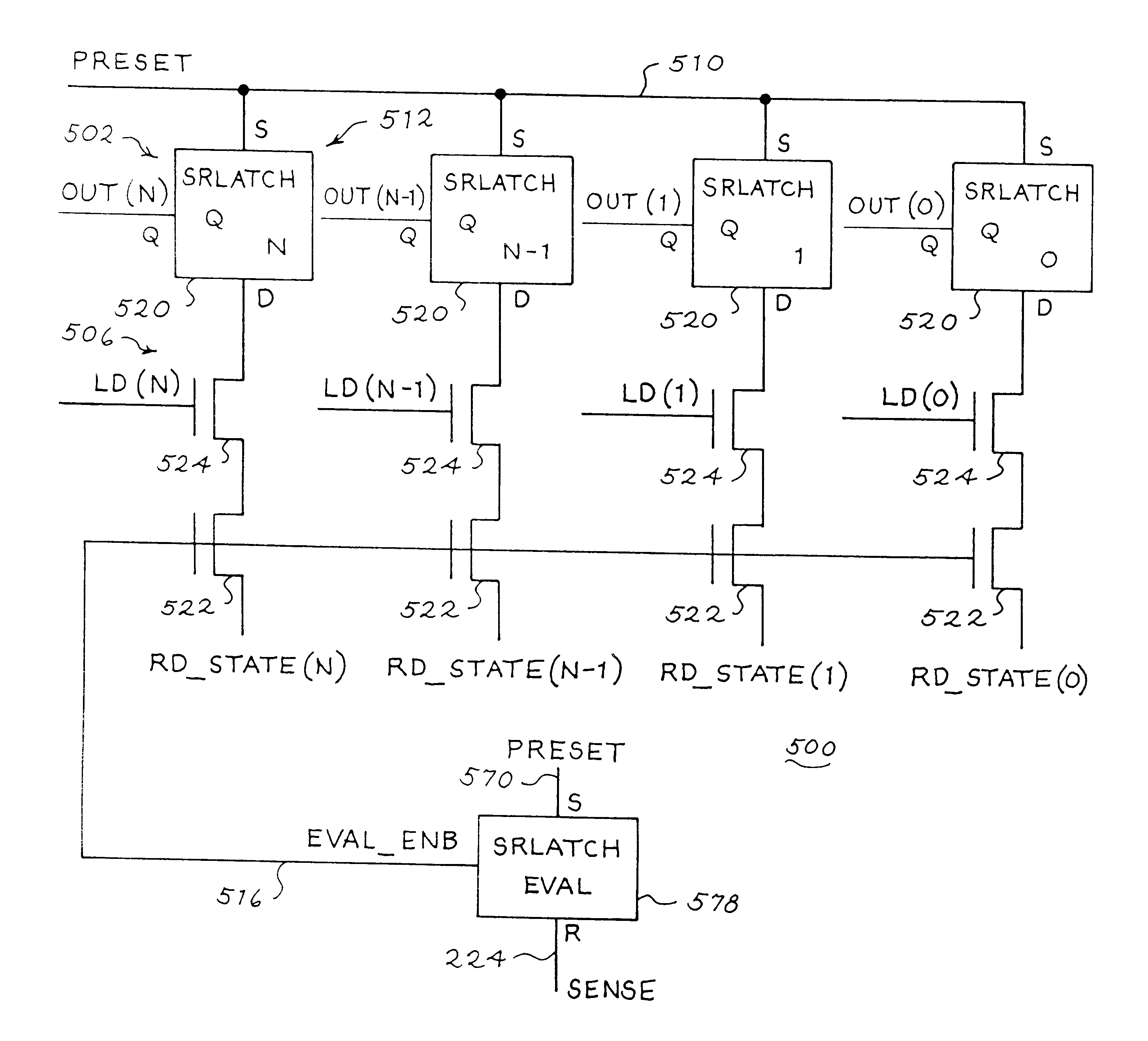
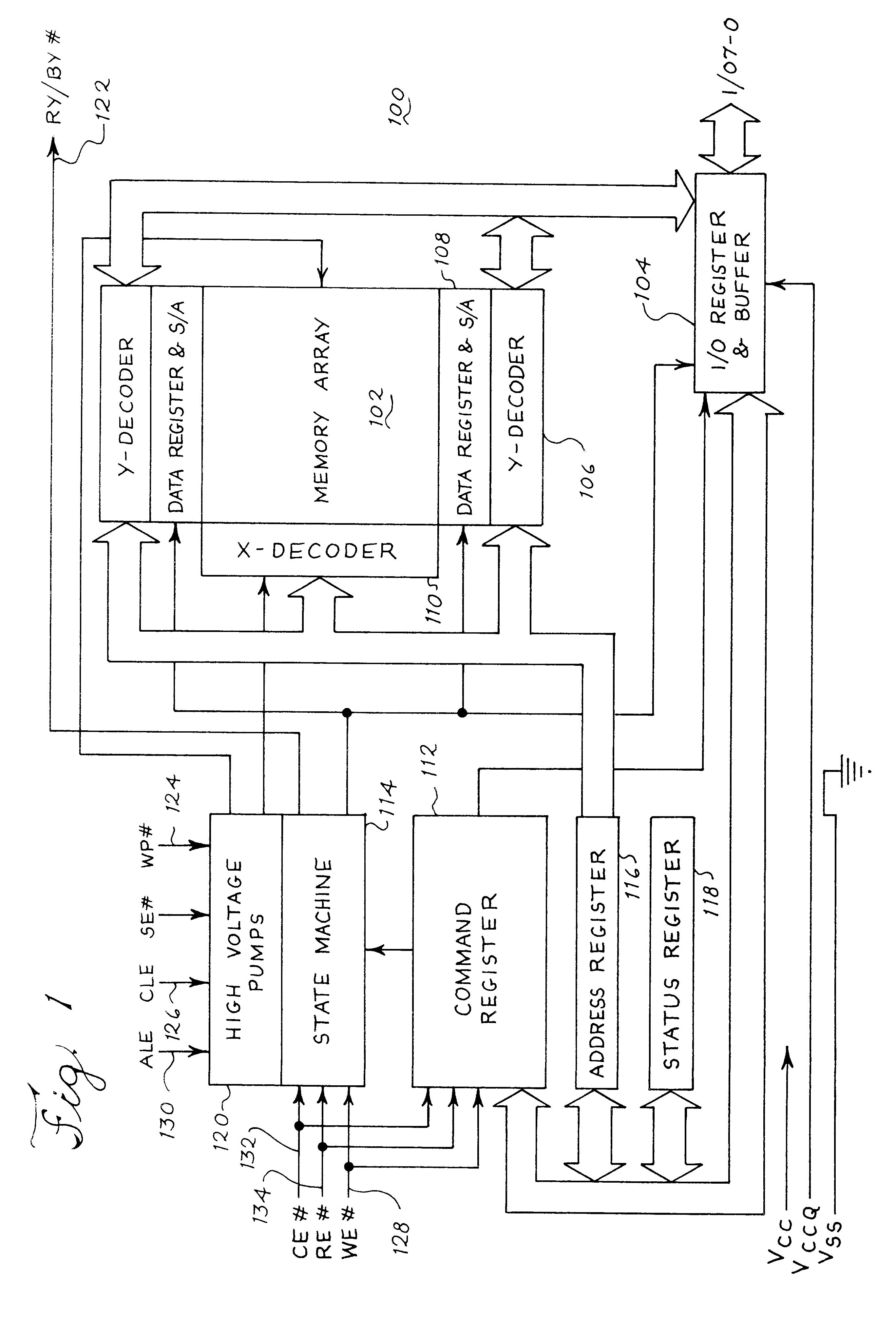
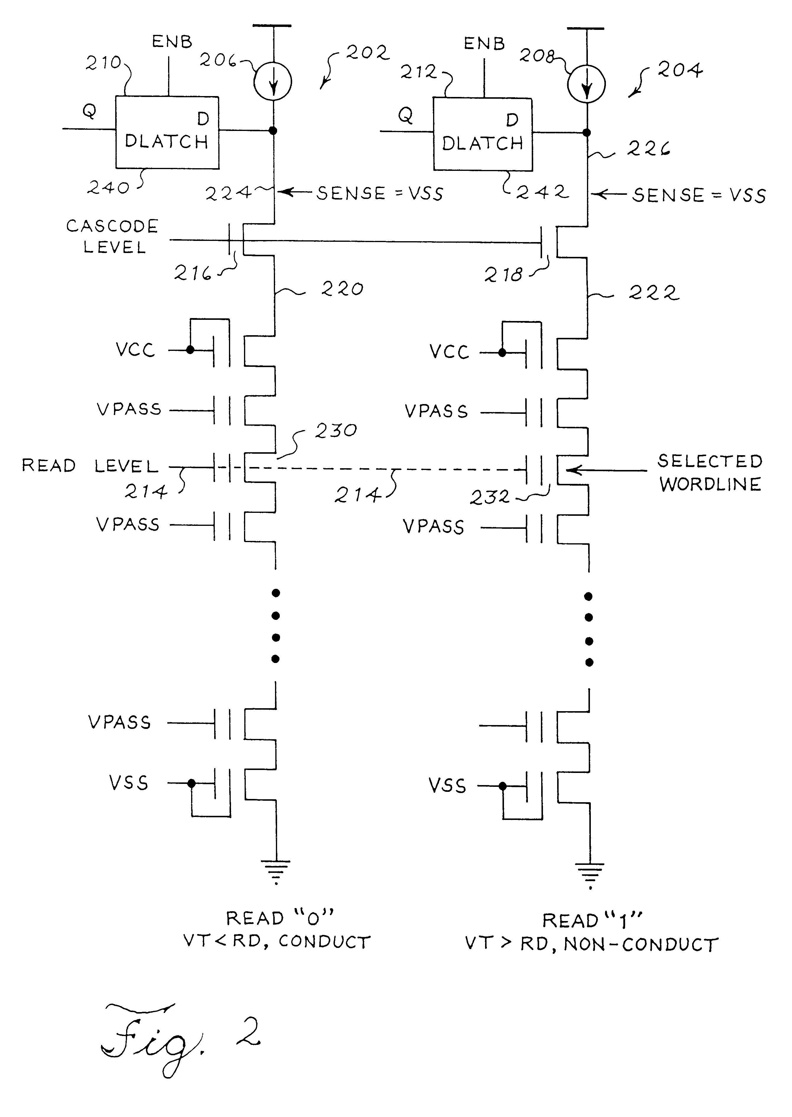
Referring now to the drawing, FIG. 1 shows a block diagram of a memory device 100. The memory device 100 in the illustrated embodiment is a NAND flash memory. However, in other embodiments, the memory device 100 may be any other suitable type of volatile memory such as random access memory (RAM) including static or dynamic RAM or nonvolatile memory such as EEPROM. Further, the memory device 100 may be an embedded memory circuit within another integrated circuit or device containing other circuitry, such as logic. As a flash memory, the memory device 100 may be written or programmed with data, read to retrieve the stored data, and erased to clear the memory device on a block-by-block basis.

In the illustrated embodiment, the memory device 100 includes a memory cell array 102, an input / output (I / O) register 104, one or more Y-decoders 106, one or more sense amplifier blocks 108 and one or more X-decoders 110. Further, the memory device 100 includes a command register 112, a state machi...


PUM


Abstract

A multi-level memory includes an array of memory cells accessible through respective word lines and bit lines a control circuit controlling embedded operations of the memory and a read voltage generating circuit to generate a descending staircase read voltage to a word line associated with a selected memory cell under control of the control circuit. The multi-level memory further includes a read circuit including a latch circuit, and a switch circuit responsive to an evaluate/enable signal to selectively store a read state signal in the latch circuit in response to a sense signal generated from application of the descending staircase read voltage to the word line associated with the selected memory cell.

Description

The present invention relates generally to memory devices. More particularly, the present invention relates to a descending staircase read technique for a multi-level cell NAND flash memory device.A variety of semiconductor memory devices have been developed for storage of information. Examples include volatile and nonvolatile memory. Nonvolatile memory provides a key advantage in that it retains stored data after power is removed from the device. One example of nonvolatile memory is flash memory. However, manufacture and operation of nonvolatile memory is generally more complex than for volatile memory. For all memory devices, important design goals include increased storage density and reduced read and write times.A conventional memory device includes an array of storage cells or memory cells. Each cell stores a single binary digit or bit of information. For example, in a flash memory, the threshold voltage of a transistor in the memory cell is adjusted according to the data store...

Claims


Application Information

Patent Timeline
IPC IPC(8): G11C16/26G11C16/06G11C11/56
CPCG11C11/5621G11C11/5642G11C16/0483G11C16/26G11C2211/5642
Inventor PARKER, ALLAN
Owner VALLEY DEVICE MANAGEMENT
Why Eureka
Try Eureka