Late-write type semiconductor memory device with multi-channel data output multiplexer

Inactive Publication Date: 2001-11-20
SAMSUNG ELECTRONICS CO LTD
View PDF2 Cites 20 Cited by
  • Summary
  • Abstract
  • Description
  • Claims
  • Application Information

AI Technical Summary

Problems solved by technology

However, in such devices there have been a number of data output errors in the high speed operation, rather than in the bypass operation.
Therefore, the aforementioned data output errors make it difficult to re

Method used


Image

  • Late-write type semiconductor memory device with multi-channel data output multiplexer
  • Late-write type semiconductor memory device with multi-channel data output multiplexer
  • Late-write type semiconductor memory device with multi-channel data output multiplexer

Examples


Embodiment Construction

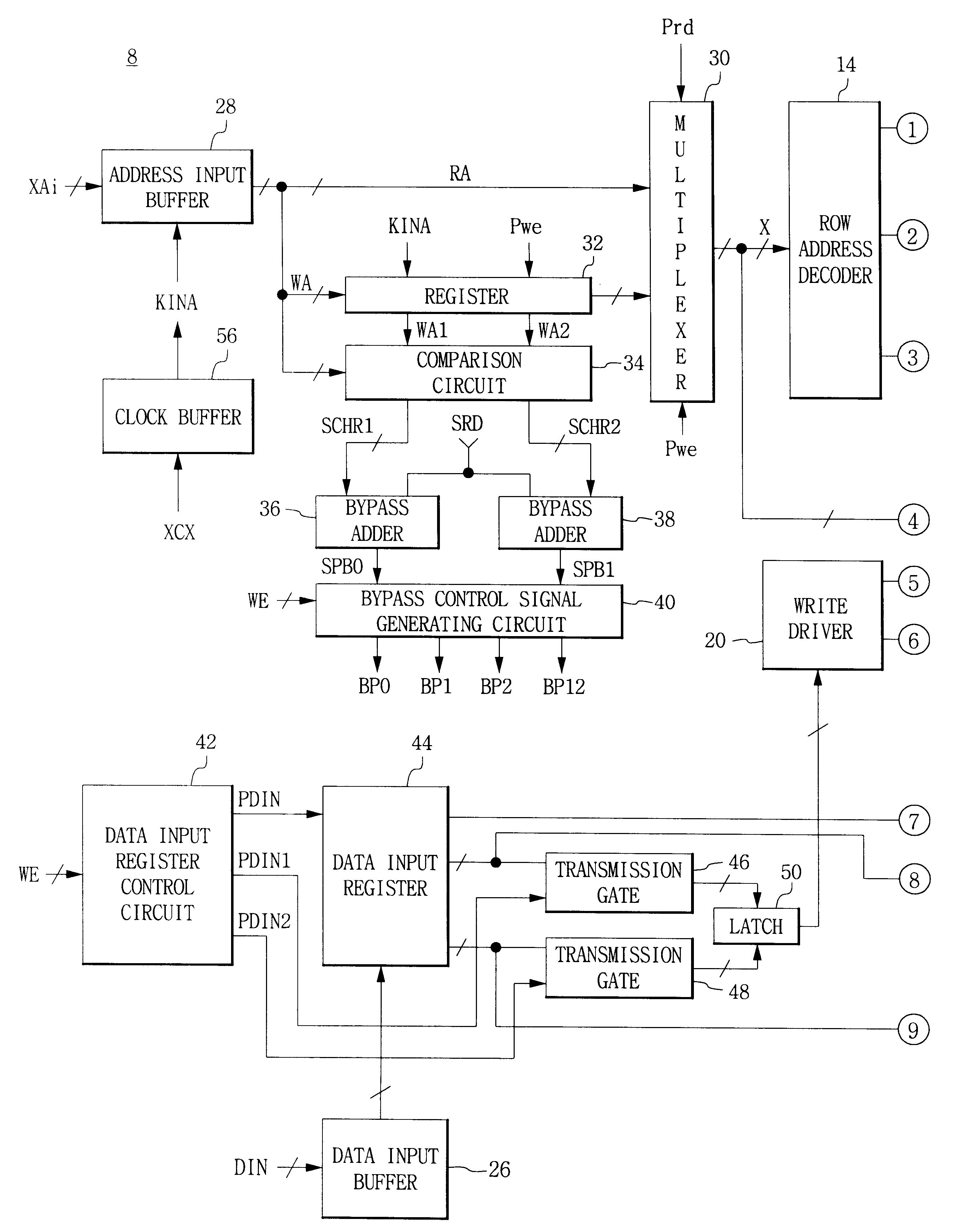
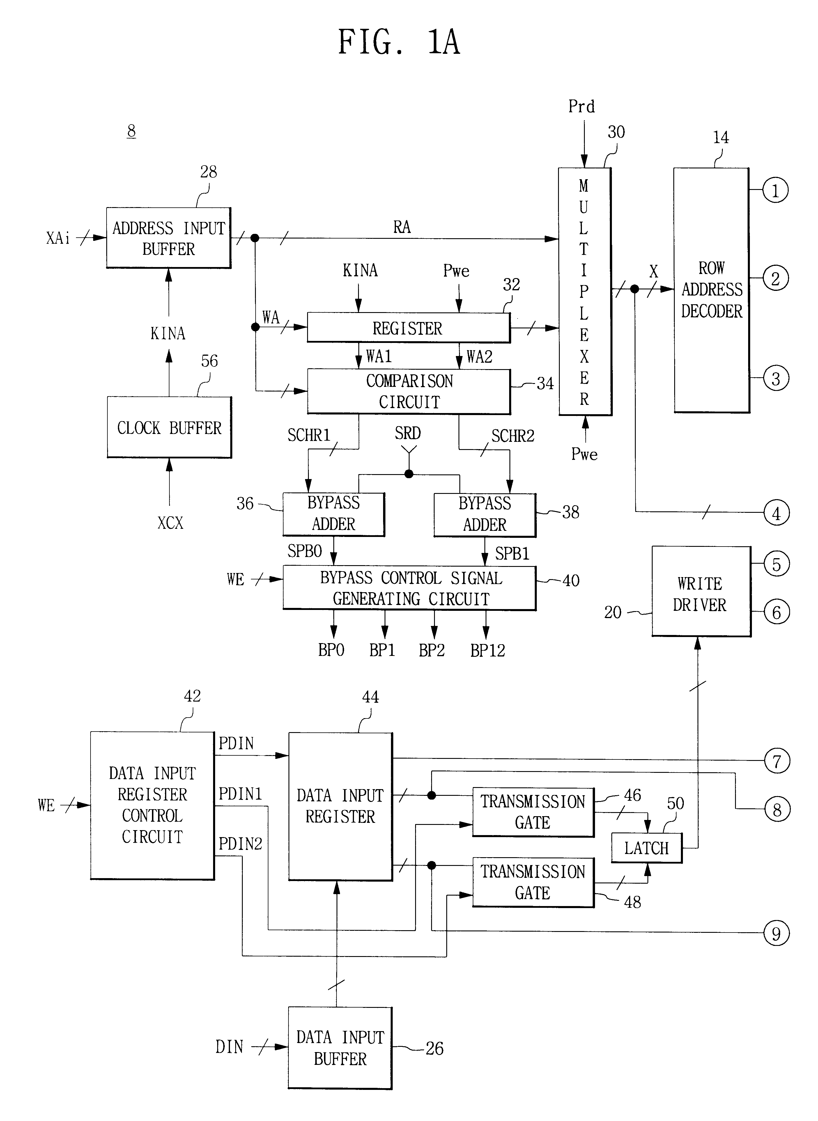
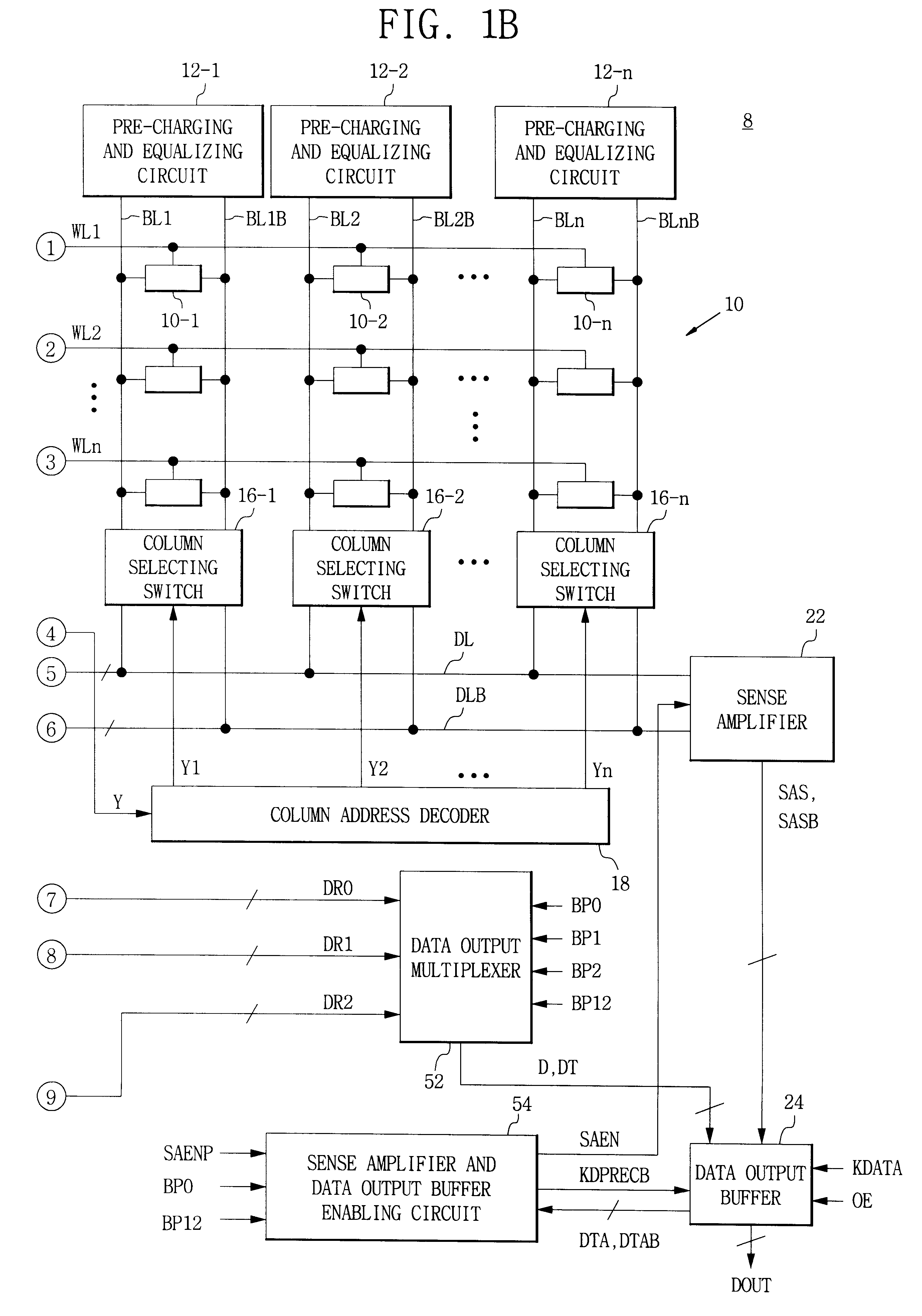
Objects and aspects of the present invention will become apparent from the following detailed description of a preferred embodiment with reference to the accompanying drawings. It should be noted that the similar or same parts in the drawings are designated with the similar or same reference numerals for convenient descriptions and understandings.

FIGS. 1A and 1B, combined form a schematic block diagram for illustrating a semiconductor memory device 8 according to the present invention. In the drawings, a late-write type semiconductor memory device having a function of bypass operation includes: memory cells 10-1, 10-2, . . . , 10-n for constructing a memory cell array 10; pre-charging, and equalizing circuits 12-1, 12-2, . . . , 12-n, row address decoder 14, column selecting switches 16-1, 16-2, . . . , 16-n, column address decoder 18, write driver 20, sense amplifier 22, data output buffer 24, data input buffer 26, address input buffer 28, multiplexer 30, register 32, comparison ci...


PUM


Abstract

A multiplexer circuit of a late-write type semiconductor memory device for selectively outputting data to be bypassed to a data output buffer is constructed with at least one or more data channels. Each data channel includes a first switch for transmitting the data in response to a first state of a bypass control signal, a latch part for latching the data output through a first switch, and a second switch for transmitting the data output from the latch part in response to a second state of the bypass control signal. Thus the circuit prevents data errors and improves time interval of cycles in bypass operation at high speed.

Description

1. Field of the InventionThe present invention relates to a semiconductor memory device, and more particularly to a late-write type semiconductor memory device like a high speed static RAM (hereinafter referred to as SRAM).2. Description of the Prior ArtA late-write type SRAM is one of a variety of prior arts concerning a synchronous type semiconductor memory device for high speed operations, where a total time required for write data reduces, resulting in an effect of improving margin of a write operation. One such SRAM is disclosed in U.S. Pat. No. 5,717, 653.The semiconductor memory device delays a write address input from outside for a number of cycles in the course of performing a late-write process to input to an address decoder and to select word line and bit line. After the write address is input and delayed by a number of cycles, the data input signal input from outside is transmitted to a write driver. Then, the write operation is actuated after a number of cycles. In othe...

Claims


Application Information

Patent Timeline
IPC IPC(8): G11C7/10H03K17/735G11C11/4197
CPCG11C7/1012G11C7/1051G11C7/106G11C7/1069G11C7/1078G11C7/109G11C2207/002H03K17/735
Inventor KANG, TAE-KYUNLEE, YOUNG-DAE
Owner SAMSUNG ELECTRONICS CO LTD
Why Eureka
Try Eureka