

Process and structure for an interlock and high performance multilevel structures for chip interconnects and packaging technologies
a multi-level structure, interlocking technology, applied in the direction of cameras, instruments, cameras, etc., can solve the problems of wiring defects, blistering, other defects, voids or seams in the wiring,
- Summary
- Abstract
- Description
- Claims
- Application Information
AI Technical Summary
Problems solved by technology
Method used
Image

Examples
Embodiment Construction
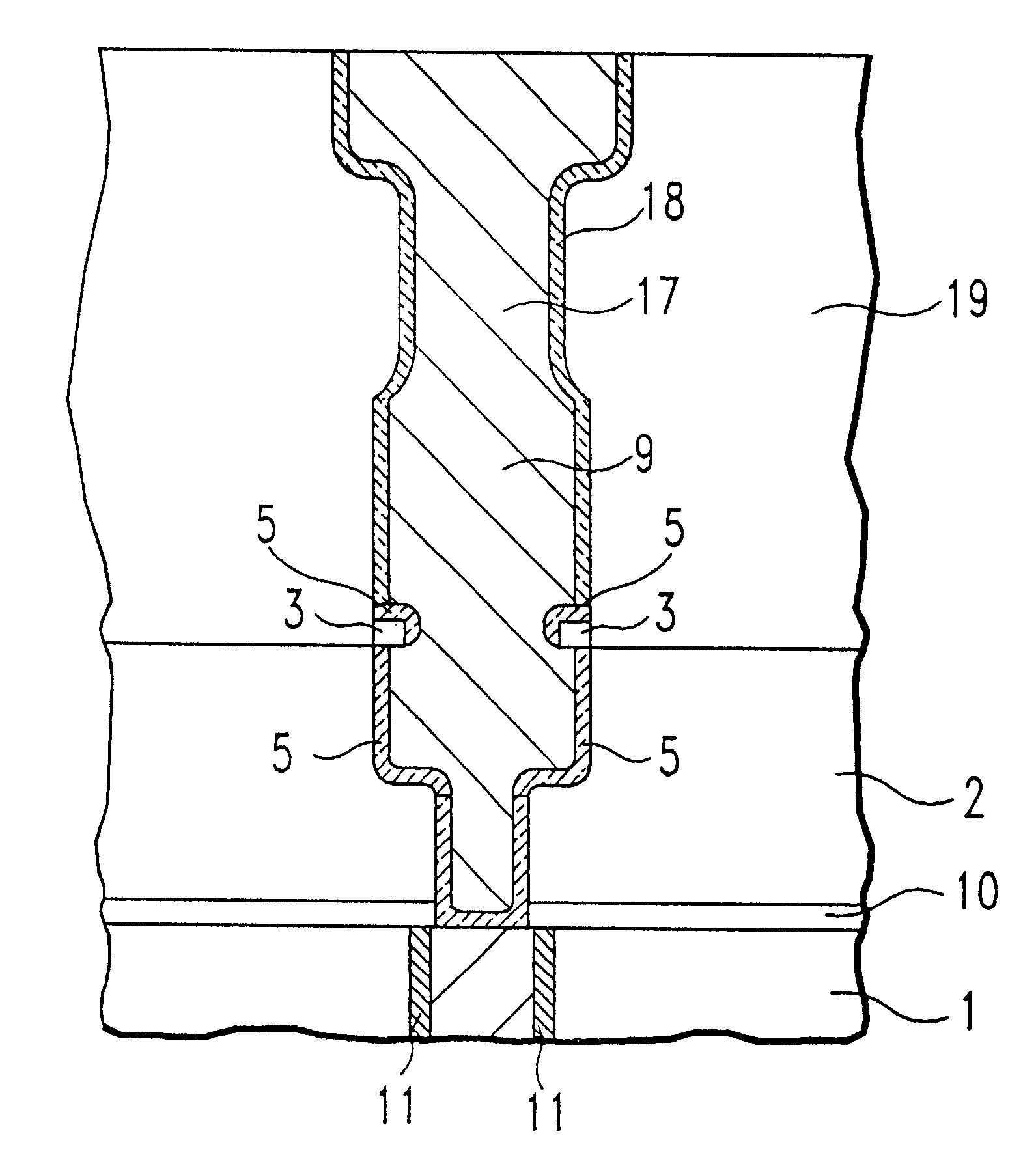
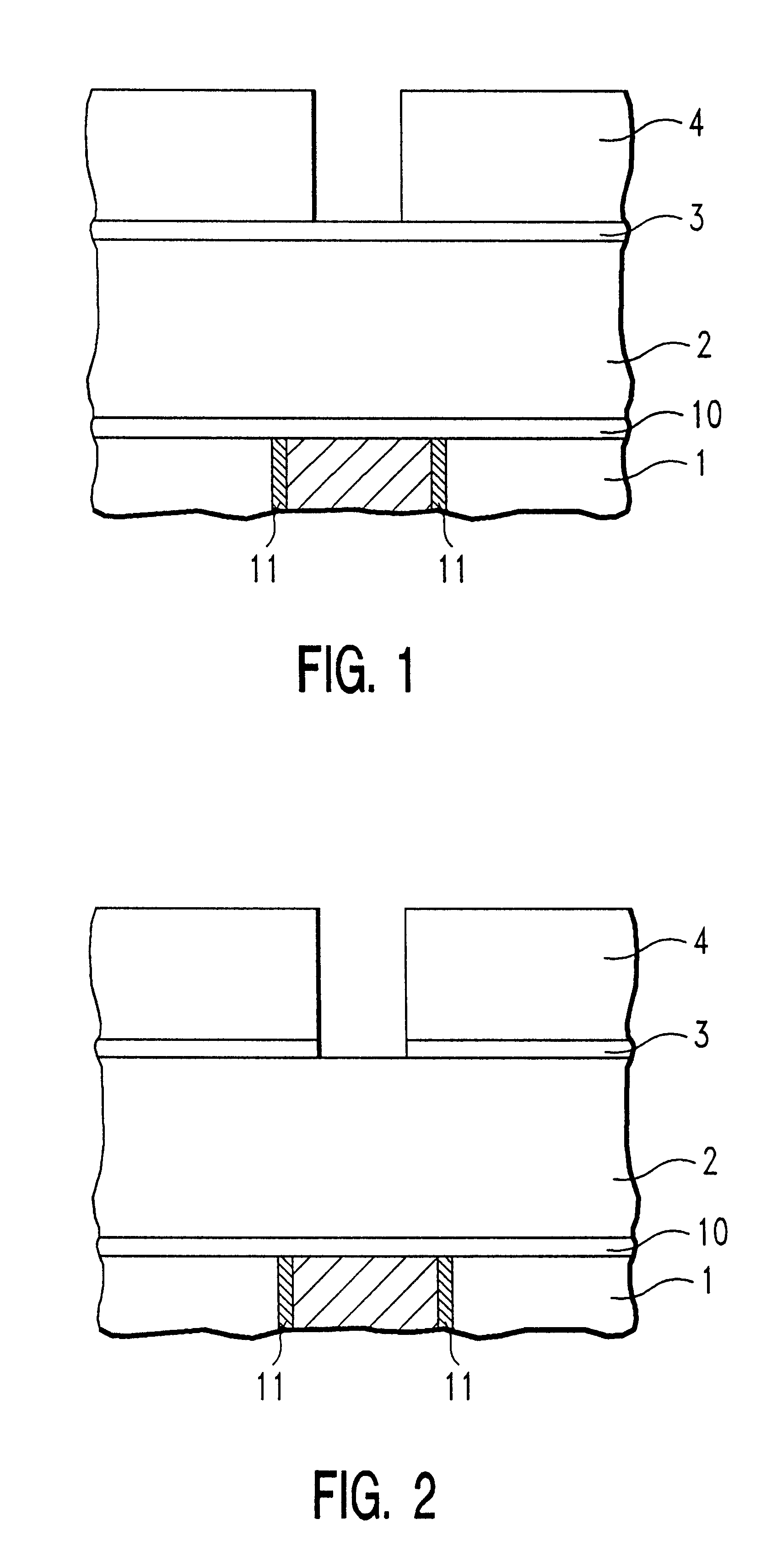
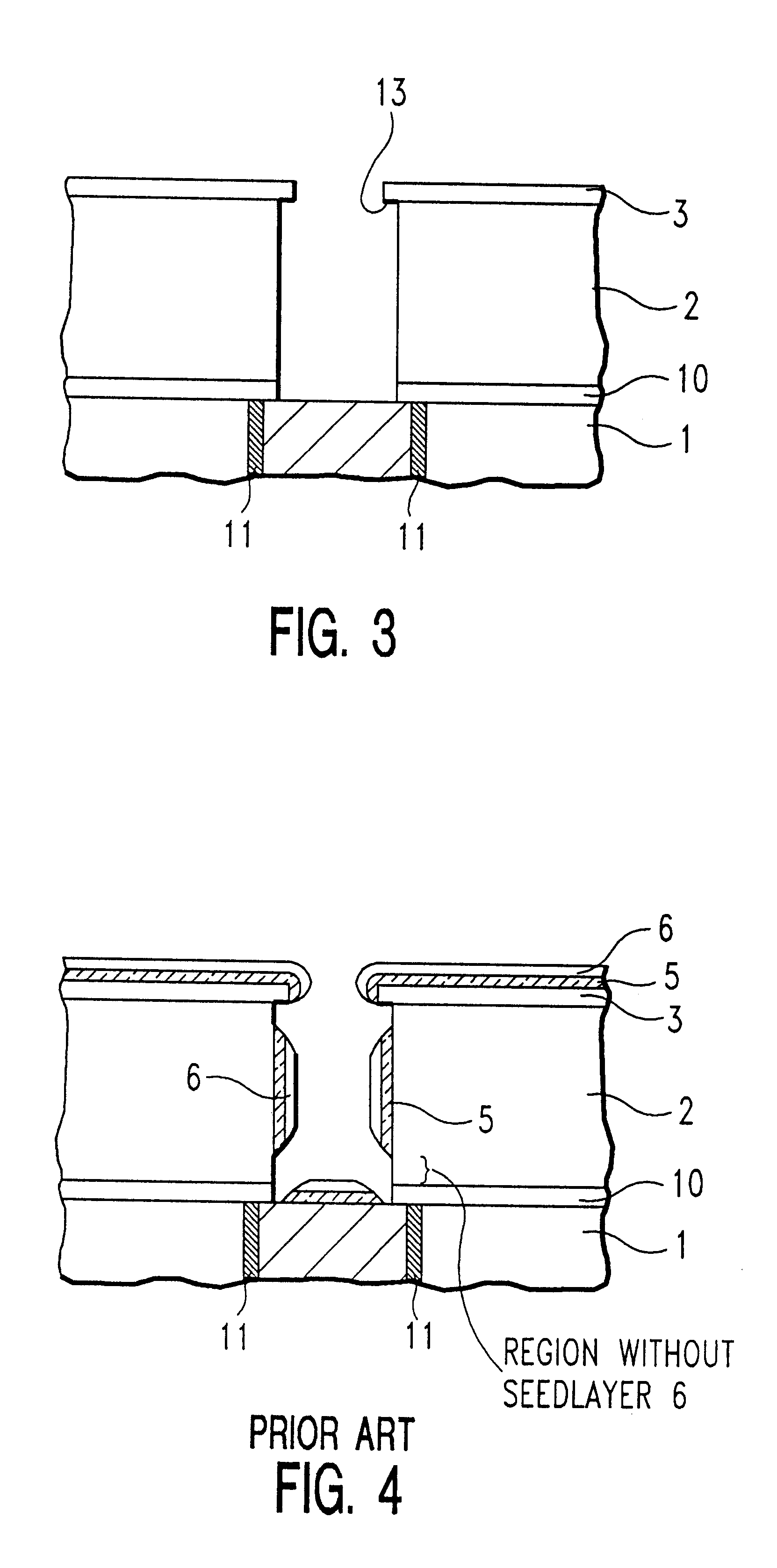
In order to facilitate an understanding of the present invention, the embodiment discussed will be directed to a Damascene plating process in which plating is carried out over a substrate such as a semiconductor, flat panel or packaging substrate.
A schematic representation of the process of the present invention is illustrated in FIGS. 1-3 and 7-17.
In particular, a layer of a first dielectric 2 is deposited over the semiconductor substrate or wafer 1. See FIG. 1. The dielectric layer 2 typically has a dielectric constant of less than 4. However, for certain applications, the dielectric constant of the dielectric layer 2 is greater than 10. As illustrated in FIG. 1, also included between the substrate 1 and dielectric layer 2 is an interlevel dielectric layer 10. Also, the substrate 1 includes lower level wiring 11. The interlevel dielectric layer is typically a silicon dioxide, silicon nitride, silicon oxynitride or alumina.
The preferred dielectric layer 2 is a polyimide. Polyimides...
PUM
| Property | Measurement | Unit |
|---|---|---|
| Electrical conductor | aaaaa | aaaaa |
| Dielectric constant | aaaaa | aaaaa |
Abstract
Description
Claims
Application Information