Circuit board for organic electroluminescent panel, method of manufacture, and electroluminescent panel

a technology of electroluminescent panels and circuit boards, which is applied in the manufacture of electrode systems, electric discharge tubes/lamps, and discharge tubes luminescent screens, etc., can solve the problems of difficult control uniform directions, difficult to carry out vapor deposition while rotating the substrate, and limited linear anode patterns

Inactive Publication Date: 2002-01-15
TOPPAN PRINTING CO LTD
View PDF24 Cites 65 Cited by
  • Summary
  • Abstract
  • Description
  • Claims
  • Application Information

AI Technical Summary

Benefits of technology

The substrate for an organic EL display element in a preferred embodiment of the first aspect can also be manufactured by utilizing a plurality of color filters arranged on a support. To be more specific, the particular substrate can be manufactured by arranging a plurality of color filters apart from each other on a support to form rows and columns of the color filters; forming a plurality of first electrode lines apart from each other on the color filters in a manner to extend in the row direction of the color filters; forming a negative photoresist layer on the first electrode lines; for the negative photoresist layer, applying, simultaneously or one before the other, a first light exposure to first regions corresponding to the top portions including eaves of the partition walls, and a second light exposure, with the color filters used as a mask, to second regions corresponding to the bottom portions of the partition walls positioned between adjacent columns of the color filters and third regions positioned between adjacent rows of the color filters, from rear side of the support; and developing the non-exposed portion to form partition walls connected to each other by a connection band corresponding to the third region.

Problems solved by technology

In this method, however, it is difficult to carry out the vapor deposition while rotating the substrate and to control uniformly the directions of the vapor deposition beams over a large area.
In addition, the anode pattern is limited to a linear pattern.
In this case, deposition takes place also on the side wall of the partition wall, leading to possibility of short-circuiting between the two electrodes.
It follows that the method using an inversely tapered partition wall is not adapted for the vapor deposition on a substrate having a large area.
On the other hand, complex steps are required for forming a partition wall having a T-shaped cross section.
Further, since there is a clearance between the partition wall and the organic EL medium layer, a difficulty is brought about if vapor deposition of the organic EL medium and the second electrode material are carried out by using the partition wall.
As a result, the second electrode is brought into direct contact with the first electrode, leading to short-circuiting that impairs the normal operation of the device.
However, formation of the insulating layer makes the manufacturing process complex.
Further, since the edge portion of the organic EL medium layer / second electrode line is exposed to the outside, deterioration tends to take place from the edge portion.
A second problem relating to the organic EL display element is that the resistance of the anode line is increased as the anode line is made finer.
As a result, a high driving voltage is required.
In this case, however, the height of the conductive metal line is limited by the height of the transparent electrode line, making it difficult to further decrease the resistance of the anode line, though the resistance can be lowered to some extent.
However, since patterning of a transparent electrode is required in this method, the manufacturing process is rendered complex.
Also, what should be particularly pointed out in this case is that, when the transparent electrode material is patterned with an etchant, the metal wiring is unavoidably corroded by the etchant.
However, if a color display is to be obtained by the particular construction, it is impossible to obtain display of pure colors because colors are mixed.
A third problem relating to the organic EL display element is that the organic EL medium layer and the second electrode line are deteriorated.
However, some problems are brought about in the case of using a cover.
As a result, the organic EL medium layer or the second electrode line is deteriorated.

Method used


Image

  • Circuit board for organic electroluminescent panel, method of manufacture, and electroluminescent panel
  • Circuit board for organic electroluminescent panel, method of manufacture, and electroluminescent panel
  • Circuit board for organic electroluminescent panel, method of manufacture, and electroluminescent panel

Examples


third embodiment

A substrate for an organic EL display element according to the present invention will now be described with reference to FIG. 25.

As shown in FIG. 25, a plurality of striped first electrode lines 12 (anode lines in this embodiment) are formed on a support 11 made of a light-transmitting insulating material such as quartz, glass or a plastic material, preferably a transparent material. Further, it is desirable to form a plurality of striped auxiliary electrode lines 91 in a region between an edge of the support and a region surrounding the first electrode lines. These auxiliary electrode lines 91 are formed apart from the first electrode lines 12 in a manner to extend from within a region surrounded by a frame 92 described later to the outside of the frame 92. Naturally, the auxiliary electrode lines 91 cross the frame 92 and can be used as electrodes that are connected to second electrode lines described later. FIG. 25 shows that the first electrode lines 12 are arranged a predetermi...

example 1

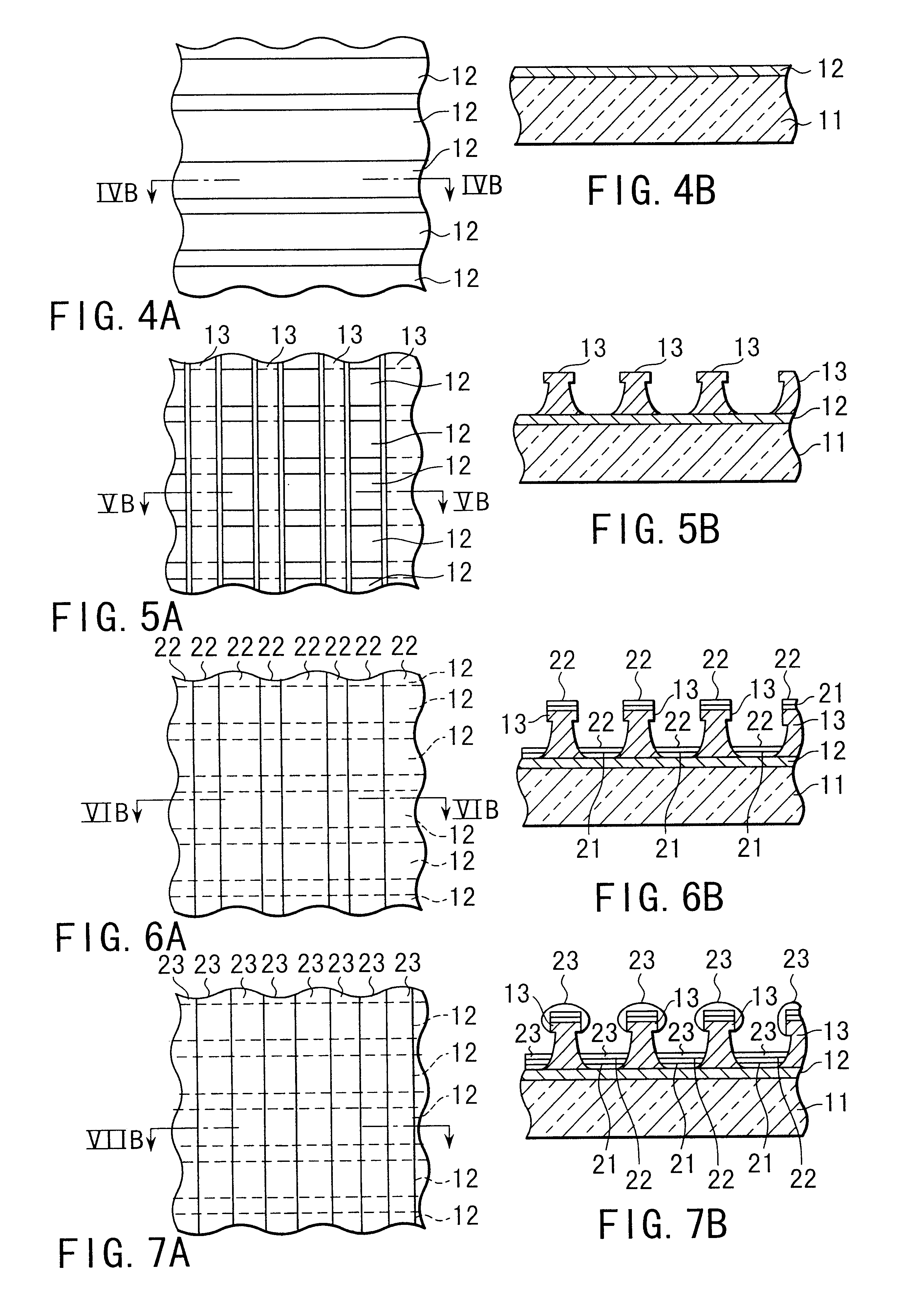
A substrate for an organic EL display element and an organic EL display element were prepared in this Example by the methods described previously in conjunction with FIGS. 4A to 7B.

In the first step, an ITO layer for the first electrode line was formed on a glass support 11 by means of sputtering. Then, for improving both the transparency and electrical conductivity of the first electrode line, a heat treatment was applied to the ITO layer within an air atmosphere so as to crystallize the ITO layer.

Then the ITO layer was patterned by photolithography and wet etching so as to form the first electrode line 12 (see FIGS. 4A and 4B).

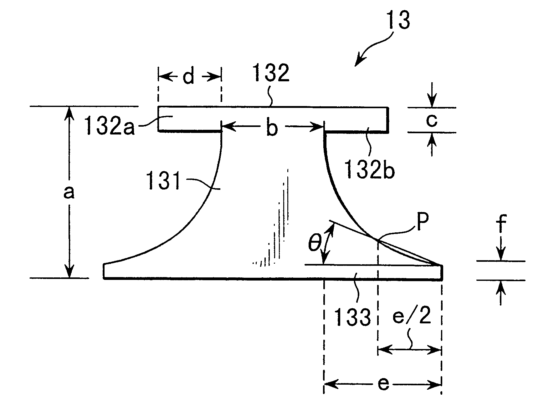
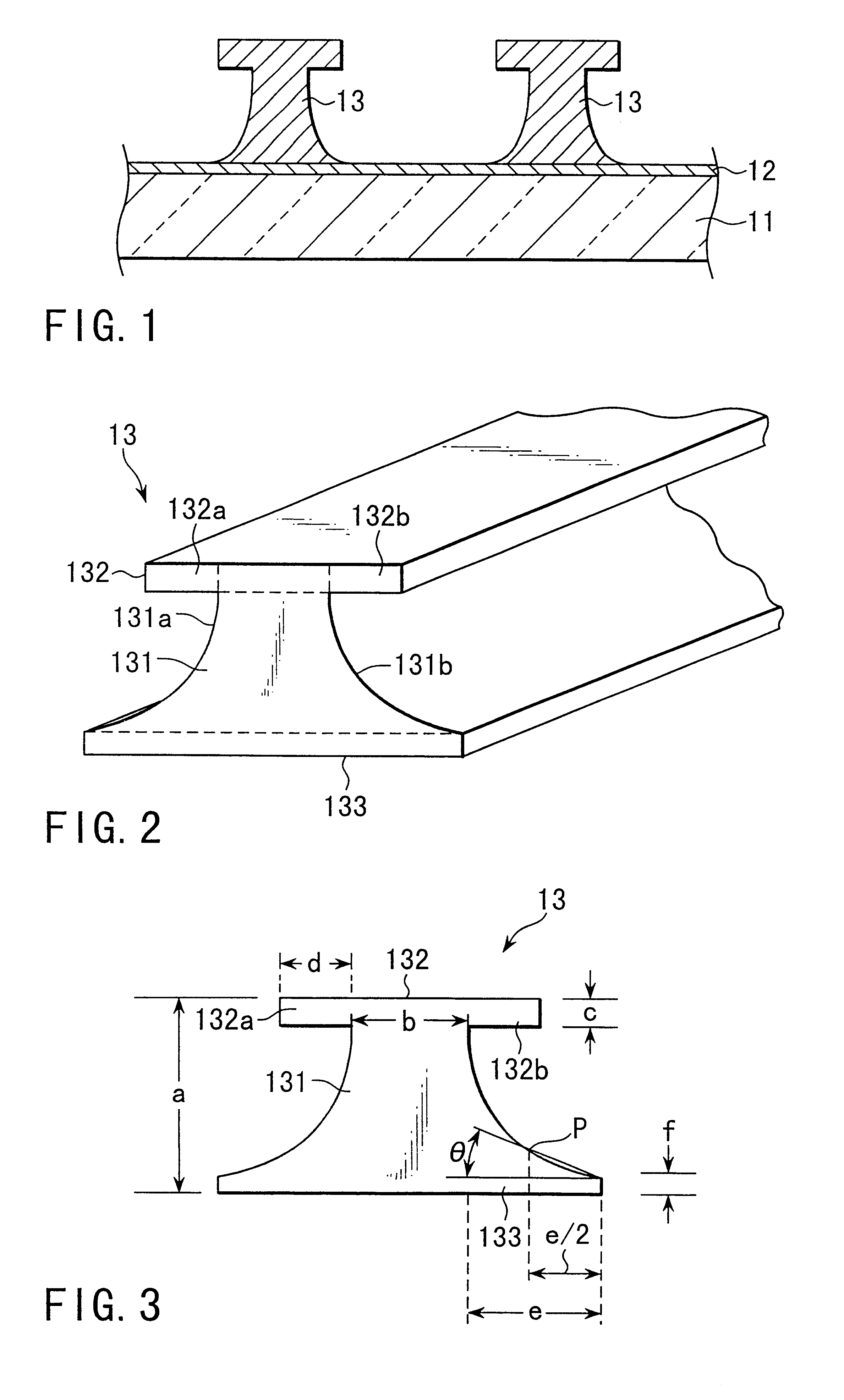
In the next step, the support 11 having the first electrode line 12 formed thereon was coated with a negative photosensitive resin having fine graphite particles acting as a black coloring matter dispersed therein, followed by pre-baking, exposing to light, developing, and post-baking the photosensitive resin layer to form partition walls 13 each having eave...

example 2

A substrate for an organic EL display element and an organic EL display element were prepared as in Example 1, except that a triazine-based organic UV-absorbing substance was used in place of the fine black graphite particles. FIG. 28 is an SEM photo showing the partition wall of the substrate for the display element thus prepared. The display element was found to be substantially equal in performance to the element prepared in Example 1.


PUM


Abstract

A substrate for an organic electroluminescence display element comprises a support (11), a plurality of first electrode lines (12) arranged apart from each other on the support (11), and a plurality of partition walls (13) arranged apart from each other and extending in a direction to cross the first electrode lines (12). Each of the partition walls (13) has eaves in an upper portion and flared side surfaces in a lower portion.

Description

The present invention relates to a substrate for an organic electroluminescence display element, which is a light emission type display for a domestic television receiver and a terminal display device for a high information processing, a method of manufacturing the same, and an organic electroluminescence display element.In the following description, the "electro-luminescence" element is often referred to as "EL" element.An organic EL display element, which is one of flat panel type display devices, is constructed basically such that an organic EL medium layer is sandwiched between a first electrode (anode or cathode) and a second electrode (cathode or anode). Light is emitted by allowing an electric current to flow between the two electrodes. The organic EL display element is of a self-light emission type and, thus, exhibits a high brightness and a wide viewing angle. In addition, the display element can be driven under a low voltage. In general, each of the first and second electr...

Claims


Application Information

Patent Timeline
Patent Type & Authority Patents(United States)
IPC IPC(8): H01L27/28H01L27/32H05B33/10H05B33/12H05B33/22
CPCH01L27/3283H01L51/5246H05B33/22H05B33/10H05B33/12H01L51/525H10K59/173H10K50/8428H10K50/8426
Inventor QIAN, YIFANISHIZAKI, MAMORUITOI, TAKESHITANI, MIZUHIROMINATO, TAKAOITO, YUICHIKAI, TERUHIKO
Owner TOPPAN PRINTING CO LTD
Why Eureka
Try Eureka