Manufacture method for semiconductor inspection apparatus

a manufacturing method and semiconductor technology, applied in semiconductor/solid-state device testing/measurement, semiconductor/solid-state device details, instruments, etc., can solve the problems of difficult mass production of inexpensive probe structures, difficult to dispose of a number of probes on a substrate, and long time-consuming to align and fix each probe with high precision

Inactive Publication Date: 2002-03-19
HITACHI LTD
View PDF4 Cites 42 Cited by
  • Summary
  • Abstract
  • Description
  • Claims
  • Application Information

AI Technical Summary

Problems solved by technology

With the probe structure shown in FIG. 13, it takes a long time to align and fix each probe with a high precision, and mass production of inexpensive probe structures is difficult.
It is therefore difficult to dispose a number of probes on a substrate, and the number of electrode pads or chips capable of being inspected collectively at one time is limited.
Further, since the length of each probe is as long as about several tens mm, the parasitic capacitance of each probe is large so that it is practically impossible to inspect a high speed device of about 100 Mhz.
Therefore, the probe tip is fast to be abraded, the life time (durable inspection times) of the probe is short, and electrode pad dusts generated during scribing may contaminate the semiconductor device manufacture environment.
If there is a variation in warp of test wafers or in height of probes, it is difficult to absorb each distance variation between the probe and a corresponding electrode pad.
Therefore, in the burn-in inspection at a high temperature of about 150.degree. C., there is a large difference of linear expansion coefficient between the probe and test wafer, so that position misalignment may exist between the probe and the electrode pad positioned remotely from the center of the test wafer.
It is therefore difficult to align probes at a fine pitch corresponding to the positions of electrode pads of a test wafer, i.e., difficult to form a plurality of probe needles each being elastically deformable.
Therefore, a manufacture yield is low and the height of respective probes is irregular.
However, this approach does not consider a variation in thicknesses of diaphragms.
If a diaphragm having a variation in warp or thickness is deformed, the height of the contact probe cannot be controlled.
Conversely, if the pressure force is too large, the probe may move deep under the pad and the test wafer may be broken.
The area capable of forming external contact terminals is therefore limited, and it is difficult to electrically connect a number of probes to the external.
It is difficult to perform a broad area simultaneous inspection, such as inspection of all electrode pads of a test wafer collectively at one time.

Method used


Image

  • Manufacture method for semiconductor inspection apparatus
  • Manufacture method for semiconductor inspection apparatus
  • Manufacture method for semiconductor inspection apparatus

Examples


Embodiment Construction

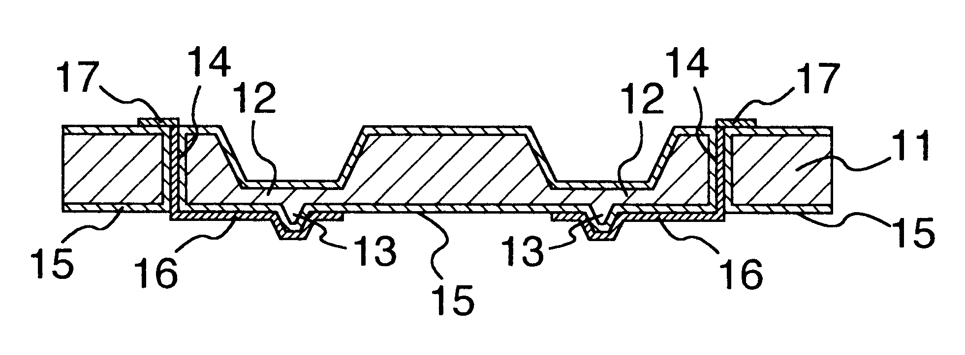
Embodiments of the invention will be described with reference to the accompanying drawings. FIG. 1 is a cross sectional view of the structure of an inspection wafer of a semiconductor inspecting apparatus according to an embodiment of the invention.

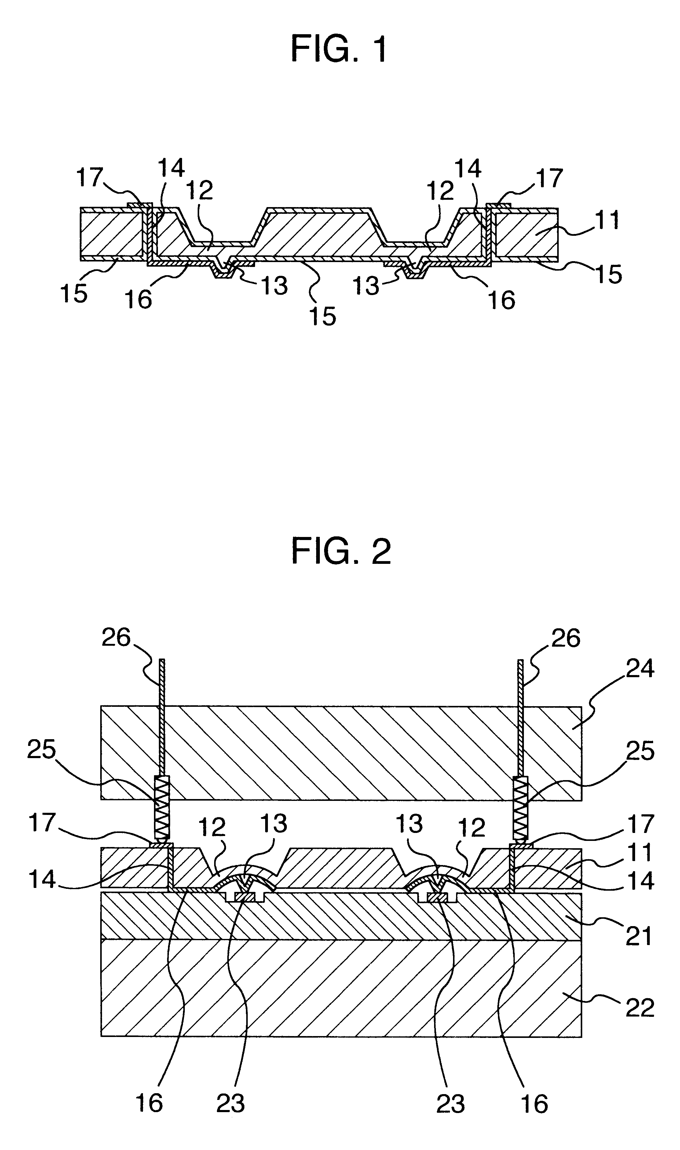
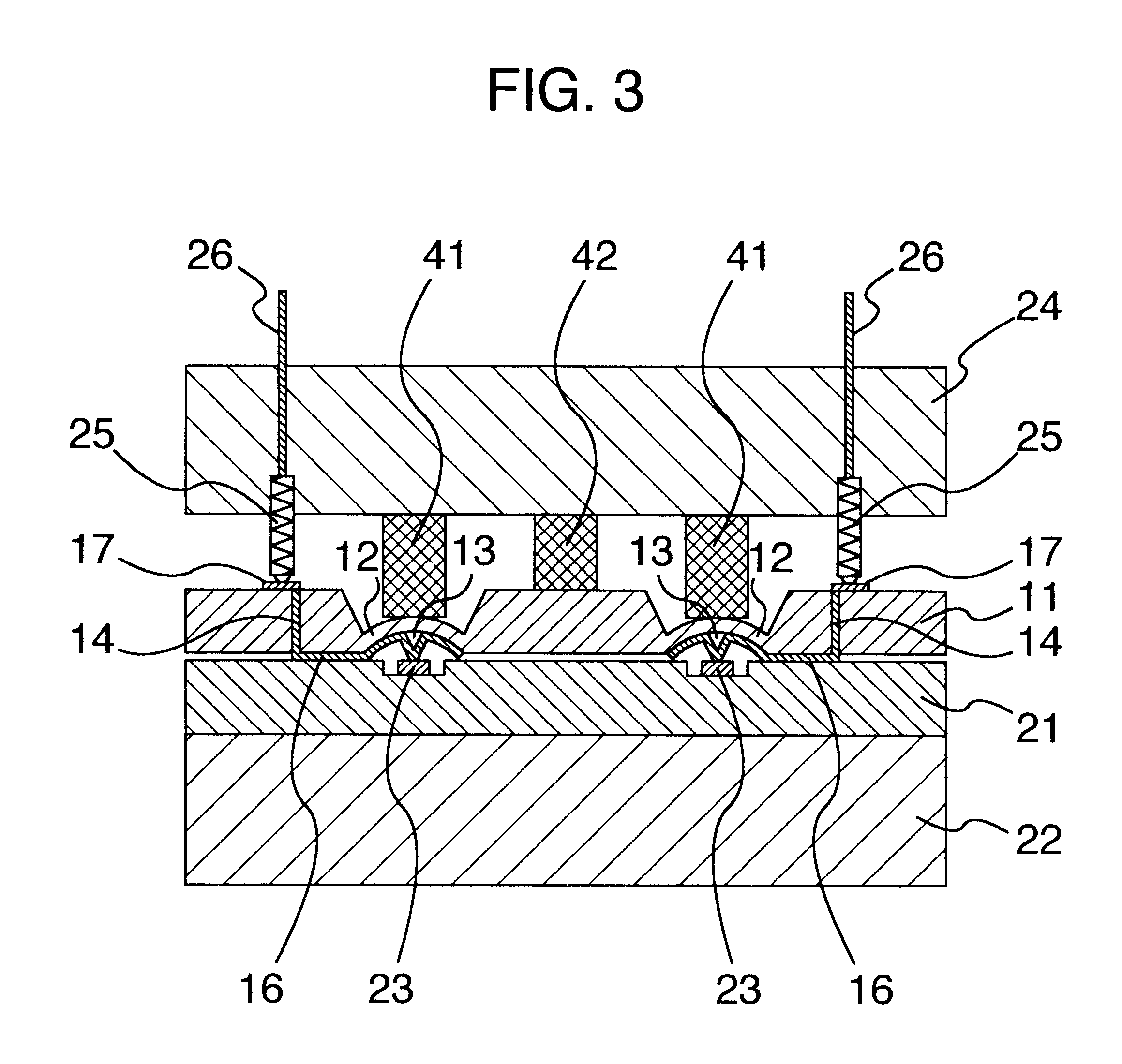
An inspection wafer 11 has a both-end supported beam or diaphragm (hereinafter, the term diaphragm is used) 12, probes 13, and through holes 14. The probe 13 is formed on the diaphragm 12 and projects downward from the bottom surface of the inspection wafer 11. The through hole 14 is formed as many as the number of probes 13. The whole surface of the inspection wafer 11 is covered with a silicon oxide film 15. The probe 13 and wiring lead 16 are formed on the silicon oxide film 15. The wiring lead 16 extends from the probe 13 via the through hole 14 to a secondary electrode pad 17 formed on the opposite surface of the inspection wafer 11.

FIG. 2 is a cross sectional view showing the structure of a semiconductor inspection apparatus accordi...


PUM


Abstract

A semiconductor inspection apparatus which is possible to inspect a plurality of semiconductor devices collectively at one time, which has conventionally been difficult because of precision or the like of probes. A method of manufacturing the semiconductor inspection apparatus comprises the steps of forming a cover film on a surface of the silicon substrate and forming a plurality of probes of a polygonal cone shape or a circular cone shape through etching after patterning by photolithography, after the cover film is removed, again forming a cover film on the surface of the silicon substrate and forming a beam or a diaphragm for each probe through etching after patterning by photolithography, after the cover film is removed, again forming a cover film on the surface of the silicon substrate and forming a through hole corresponding to the probe through etching after patterning by photolithography, and after the cover film is removed, forming an insulating film on the surface of the silicon substrate, forming a metal film on a surface of the insulating film, and forming a wiring lead through etching after patterning by photolithography.

Description

1. Field of the InventionThe present invention relates to a method of inspecting semiconductor elements or semiconductor devices formed on a wafer, and more particularly to an inspection apparatus for measuring electrical characteristics during semiconductor manufacture processes such as probing inspection and burn-in inspection.2. Description of the Related ArtManufacture processes for semiconductor elements such as ICs (Integrated Circuits) and LSIs (Large Scale Integrated circuits) are roughly classified into pre-processes until circuits are formed on a silicon wafer surface and post processes until the silicon wafer is scribed into separate chips which are sealed by resin, ceramic or the like. At a predetermined stage during the pre-process, the electrical characteristics of each circuit of a semiconductor device is inspected to judge whether each chip is good or defective. The electrical characteristic inspection is divided into probing inspection for judging conduction error b...

Claims


Application Information

Patent Timeline
Patent Type & Authority Patents(United States)
IPC IPC(8): G01R1/073G01R3/00H01L23/12H01L23/13H01L23/58G01R1/067H01L21/66
CPCG01R1/07314G01R3/00H01L23/13H01L22/32G01R1/06711G01R1/06738H01L2924/0002H01L2924/13091H01L2924/00
Inventor KOHNO, RYUJIMIURA, HIDEOENDO, YOSHISHIGEKANAMARU, MASATOSHIHOSOGANE, ATSUSHIAOKI, HIDEYUKIBAN, NAOTO
Owner HITACHI LTD
Why Eureka
Try Eureka