Patterned substrate, formation method of patterned substrate and mask for producing patterned substrate

A technology for patterning substrates and masks, applied in the field of masks, can solve the problems of high cost, complex process and high process precision requirements, and achieve the effects of improving crystal quality and luminous brightness.

Active Publication Date: 2012-11-07
HANGZHOU SILAN AZURE
View PDF5 Cites 29 Cited by
  • Summary
  • Abstract
  • Description
  • Claims
  • Application Information

AI Technical Summary

Problems solved by technology

However, the process of making steps on the patterned substrate is more complicated, and the process precision is required to be high, so the cost is high. How

Method used


Image

  • Patterned substrate, formation method of patterned substrate and mask for producing patterned substrate
  • Patterned substrate, formation method of patterned substrate and mask for producing patterned substrate
  • Patterned substrate, formation method of patterned substrate and mask for producing patterned substrate

Examples


Embodiment Construction

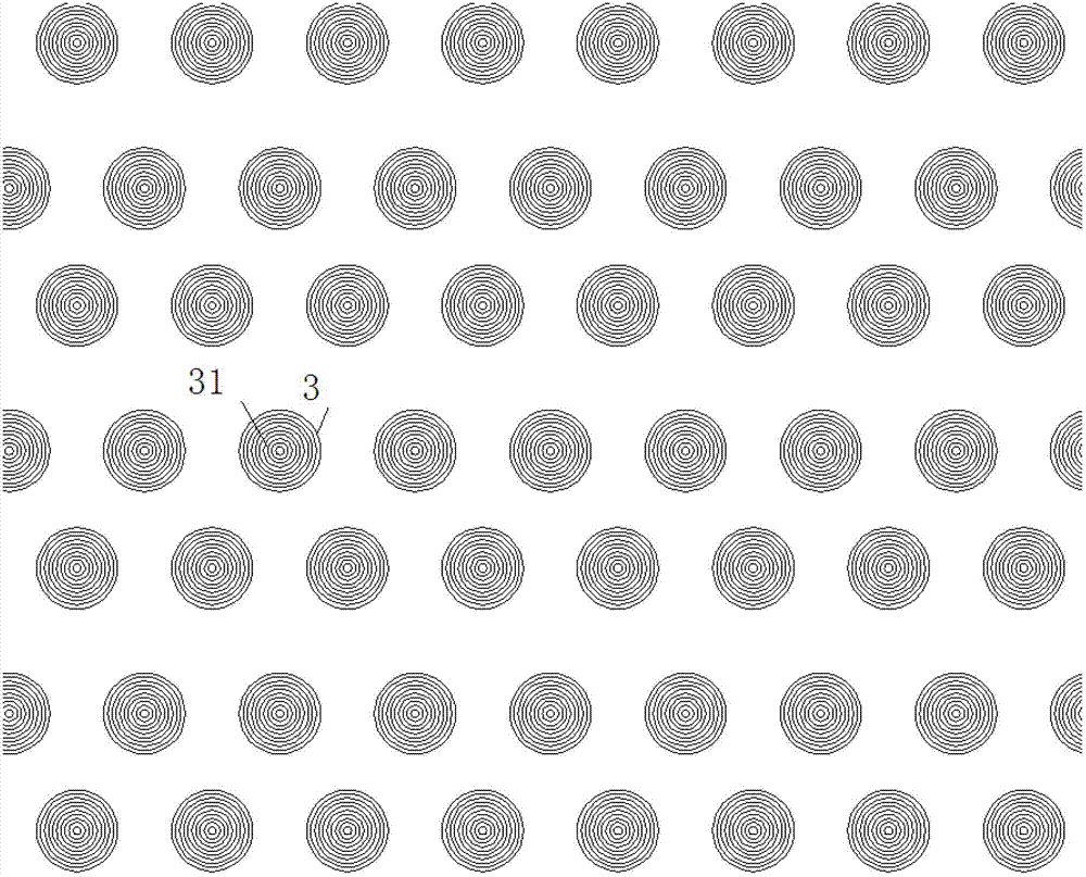
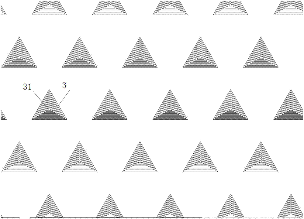
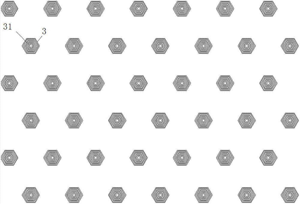
[0032] The present invention will be described in further detail below in conjunction with accompanying drawing:

[0033] In the following description, numerous specific details are set forth in order to provide a thorough understanding of the present invention. However, the present invention can be implemented in many other ways different from those described here, and those skilled in the art can make similar extensions without violating the connotation of the present invention, so the present invention is not limited by the specific implementation disclosed below.

[0034] Secondly, the present invention is described in detail using schematic diagrams. When describing the embodiments of the present invention in detail, for the convenience of explanation, the cross-sectional view showing the device structure will not be partially enlarged according to the general scale, and the schematic diagram is only an example, and it should not be limited here. The protection scope of t...


PUM

PropertyMeasurementUnit
Bottom diameteraaaaaaaaaa
Heightaaaaaaaaaa
Thicknessaaaaaaaaaa

Abstract

The invention provides a patterned substrate, which comprises a substrate and a periodic pattern which is arranged above the substrate. The periodic pattern consists of m+1 circular cone frustums, elliptical cone frustums or polygonal prism frustums which are sequentially stacked in steps from bottom to top, or consists of m circular cone frustums or elliptical cone frustums which are sequentially stacked in steps from bottom to top, and one circular cone frustum, elliptical cone frustum or polygonal prism frustum. Through the microstructure of the periodic pattern, stress caused by lattice mismatch between a GaN epitaxial layer or the like and the substrate, and dislocation density in the GaN epitaxial layer or the like can be reduced, the crystal quality of the GaN epitaxial layer or the like is improved and the brightness of an LED (light-emitting diode) is better improved. The invention additionally provides a mask consisting of a circular array, elliptical array or polygonal array. The internal part of each circular, elliptical or polygonal area in the array comprises m+1 concentric circular rings, concentric elliptical rings or concentric polygonal rings with different transmittances. The invention additionally provides a method for producing the patterned substrate by using the provided mask. The method is easy to realize and the cost is low.

Description

technical field [0001] The invention relates to the technical field of semiconductors, in particular to a patterned substrate, a method for forming the same, and a mask for making the substrate. Background technique [0002] III-V nitrides mainly GaN, InGaN and AlGaN are semiconductor materials that have attracted much attention in recent years. They have a continuously variable direct band gap of 1.9eV-6.2eV, excellent physical and chemical stability, and high saturation electron migration. High efficiency and other characteristics make it the most preferred material for optoelectronic devices such as lasers and light-emitting diodes (LEDs). [0003] Nitride optoelectronic devices are usually prepared on sapphire substrates, and the lattice constants of sapphire and GaN materials differ by 15%, and the thermal expansion coefficients and chemical properties also differ greatly. The large lattice mismatch makes the defect density of the nitride epitaxial layer grown on the s...

Claims


Application Information

Patent Timeline
IPC IPC(8): H01L33/20H01L33/00G03F1/80
Inventor 丁海生李东昇马新刚江忠永张昊翔王洋李超逯永建黄捷
Owner HANGZHOU SILAN AZURE
Why Eureka
Try Eureka