Angled halo implant tailoring using implant mask

a technology of halo and implant mask, which is applied in the direction of basic electric elements, semiconductor devices, electrical equipment, etc., can solve the problems of increasing density, number, and cost, and lowering the overall cost per transistor as well as the cost of integrated circuit devices incorporating such transistors, and adding yet another layer of complexity

Inactive Publication Date: 2002-04-16
ADVANCED MICRO DEVICES INC
View PDF2 Cites 43 Cited by
  • Summary
  • Abstract
  • Description
  • Claims
  • Application Information

AI Technical Summary

Problems solved by technology

Additionally, reducing the size, or scale, of the components of a typical transistor also increases the density, and number, of the transistors that can be produced on a given amount of wafer real estate, lowering the overall cost per transistor as well as the cost of integrated circuit devices incorporating such transistors.
However, the conventional technique schematically illustrated in FIG. 3 for implanting the asymmetric P.sup.- -doped (N.sup.- -doped) angled

Method used


Image

  • Angled halo implant tailoring using implant mask
  • Angled halo implant tailoring using implant mask
  • Angled halo implant tailoring using implant mask

Examples


Embodiment Construction

Illustrative embodiments of the invention are described below. In the interest of clarity, not all features of an actual implementation are described in this specification. It will of course be appreciated that in the development of any such actual embodiment, numerous implementation-specific decisions must be made to achieve the developers' specific goals, such as compliance with system-related and business-related constraints, which will vary from one implementation to another. Moreover, it will be appreciated that such a development effort might be complex and time-consuming, but would nevertheless be a routine undertaking for those of ordinary skill in the art having the benefit of this disclosure.

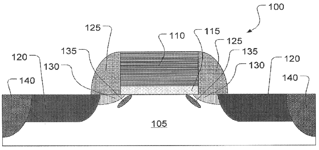
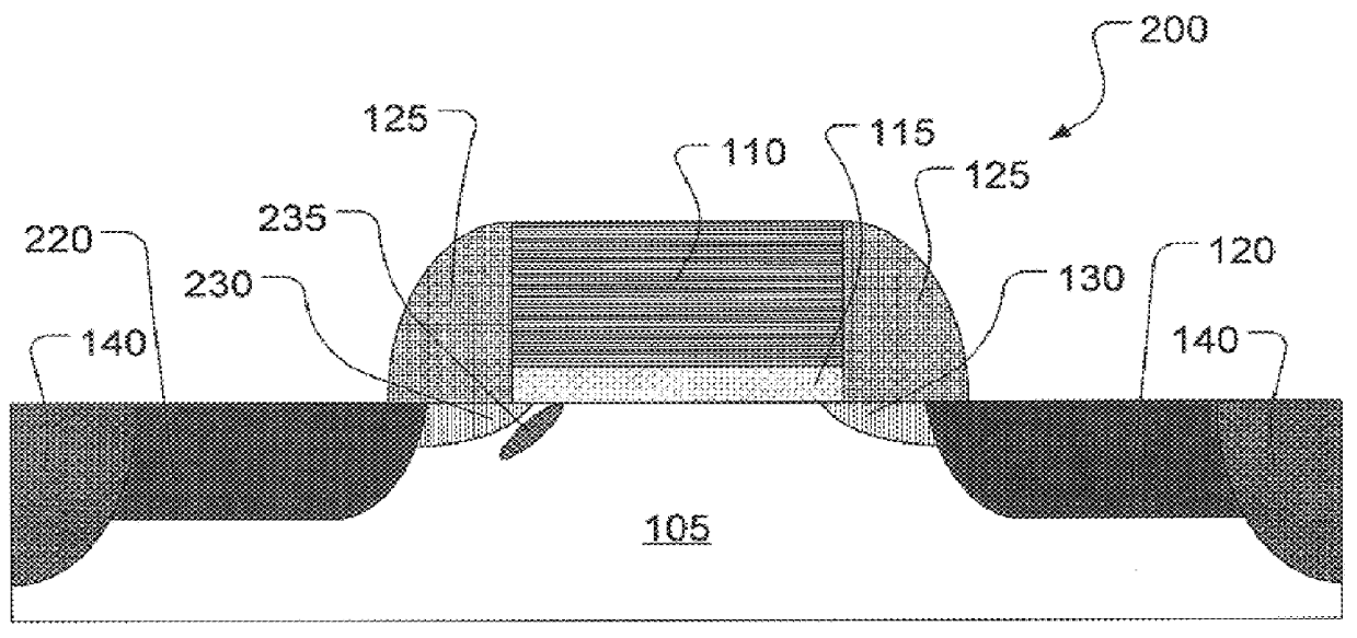
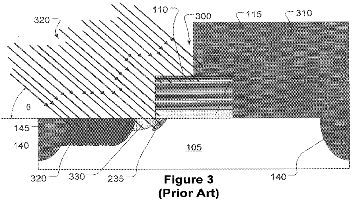
Illustrative embodiments of a method for semiconductor device fabrication according to the present invention are shown in FIGS. 5-12. Although the various regions and structures of a semiconductor device are depicted in the drawings as having very precise, sharp configurations and prof...


PUM


Abstract

A method is provided for forming a halo implant in a substrate adjacent one side of a structure, the method including forming the structure above a surface of the substrate, the structure having first and second edges and forming a mask defining a region adjacent the structure, the mask having a thickness τ above the surface and having an edge disposed a distance delta from the first edge of the structure. The method also includes implanting the halo implant at an angle alpha with respect to a direction perpendicular to the surface, wherein the tangent of the angle alpha is at least the ratio of the distance delta to the thickness τ.

Description

1. FIELD OF THE INVENTIONThis invention relates generally to semiconductor fabrication technology, and, more particularly, to a method of forming a halo implant in a substrate adjacent one side of a structure such as a gate structure of a transistor.2. DESCRIPTION OF THE RELATED ARTThere is a constant drive within the semiconductor industry to increase the operating speed of integrated circuit devices, e.g., microprocessors, memory devices, and the like. This drive is fueled by consumer demands for computers and electronic devices that operate at increasingly greater speeds. This demand for increased speed has resulted in a continual reduction in the size of semiconductor devices, e.g., transistors. That is, many components of a typical field effect transistor (FET), e.g., channel length, junction depths, gate dielectric thickness, and the like, are reduced. For example, all other things being equal, the smaller the channel length of the FET, the faster the transistor will operate. ...

Claims


Application Information

Patent Timeline
IPC IPC(8): H01L29/78H01L21/265H01L21/02H01L29/66H01L21/336
CPCH01L21/26586H01L29/7835H01L29/66659H01L29/66492
Inventor CHEEK, JON D.LUNING, SCOTT D.WRISTERS, DERICK J.
Owner ADVANCED MICRO DEVICES INC
Why Eureka
Try Eureka