
Expanded lead pitch for semiconductor package and method of electrical testing

Inactive Publication Date: 2002-04-23
TEXAS INSTR INC
View PDF12 Cites 12 Cited by
  • Summary
  • Abstract
  • Description
  • Claims
  • Application Information

AI Technical Summary

Benefits of technology

The invention provides improved apparatus and methods for testing fine lead pitch semiconductor packages. It has particular application to semiconductor surface mount packages, especially to multi-layer ceramic chip carriers of the quad flat pack type with ceramic tie bars. The invention enables an effective expansion of lead pitch for testing and the provision of test contactors exploiting this opportunity for easier as well as more precise testing.
Another object of the present invention is to provide a testing method with high alignment flexibility and contact reliability while retaining lead coplanarity and avoiding stress or damage to the delicate leads.
Another object of the present invention is to provide a method of expanding the effective lead pitch of high lead count semiconductor packages for reliable testing.
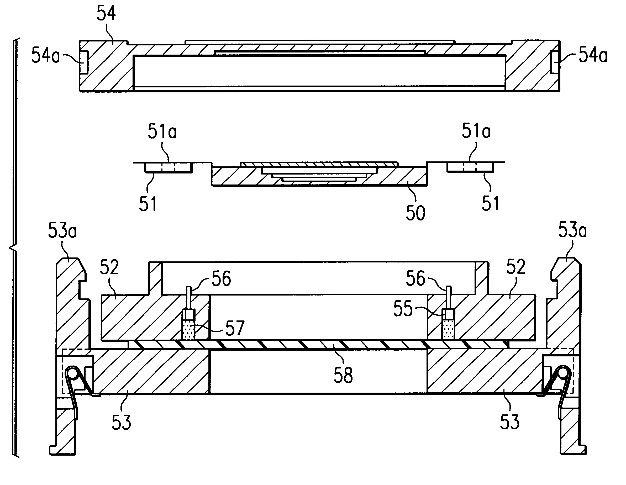
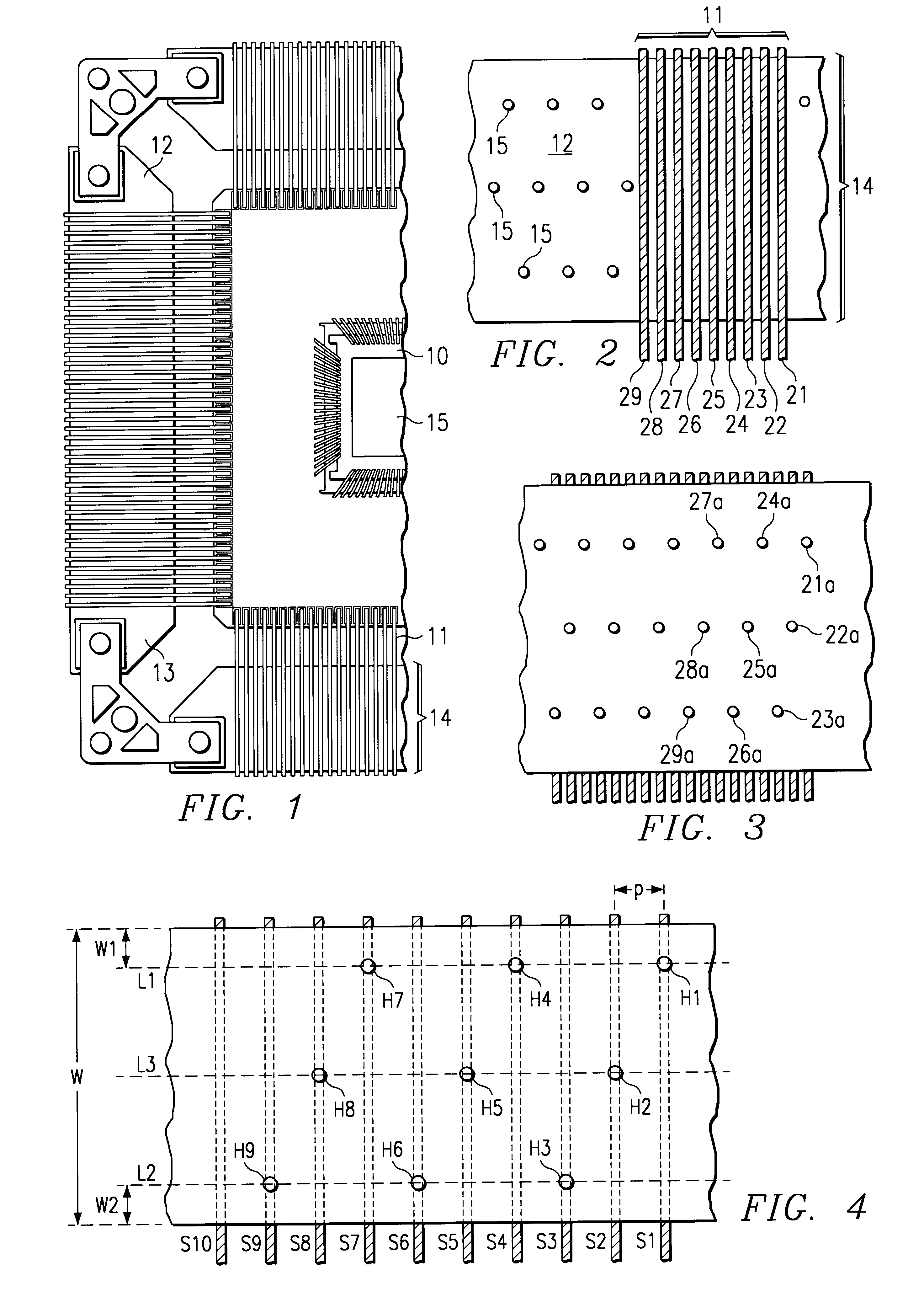
In one embodiment of the invention, the fine pitch leads of a chip carrier are supported by tie bars made of electrically insulating material, which include conductive vias arranged in a periodically staggered array. At one surface, each via contacts one lead of the package, while at an opposite surface the via is adapted to be contacted by a metal pin provided in a test contactor. The pattern of the staggering of the vias is designed so that the contacting pins are spatially separated for electrical testing, resulting in an effective lead pitch for testing expanded two-to-flour fold compared to the actual physical lead pitch.

Problems solved by technology

These trends are conflicting and have resulted in ever smaller pitch of the package leads.
Narrower and closely spaced leads, in turn, make mechanical handling more difficult due to weakened strength and tighter proximity; they also result in distortions of electrical testing due to electrical losses and stray effects.
The extra hardware of such contactors is difficult to adapt to an automated test environment.
In most applications, this limits the process to high-cost and time consuming manual test operation.
In addition, the excessive contact length of most conventional contactors and their long spring-loaded contact pins introduce a high inductance path and electrical noise into the test environment.
Furthermore, they make the contacts mechanically fragile.
Contact manipulation with lead combs or extra alignment features in conventional contactors create electrical test problems when used with high speed semiconductor devices and are subject to excessive mechanical failure and poor device alignment.
Through-hole or soldered pin methods for installation in conventional test contactors are especially cumbersome.

Method used


Image

  • Expanded lead pitch for semiconductor package and method of electrical testing
  • Expanded lead pitch for semiconductor package and method of electrical testing
  • Expanded lead pitch for semiconductor package and method of electrical testing

Examples


first embodiment

the invention as shown in FIGS. 1, 2 and 3 is implemented in the form of a single piece multilayer ceramic chip carrier of the quad flat pack with tie bar that can be used in current semiconductor device production processes and installed equipment base. The single piece multilayer ceramic chip carrier has a metallized chip mount pad onto which a semiconductor chip is attached. For the example shown in FIG. 1, the chip mount pad 10 is about 14 mm square shaped and made of ceramic with gold flash metallization (for electrical connection to ground). Electrically separate from the chip mount pad are the multitude of metal lines connecting to the lead segments 11 (which are often simply referred to as "leads"). For the example in FIG. 1, the metal lines are laid out on double layer ceramic so that they connect to 288 leads arranged on four sides, with 72 leads on each side, and are made of gold or copper with gold flash. The leads are substantially arranged in a plane; as defined herein...


PUM


Abstract

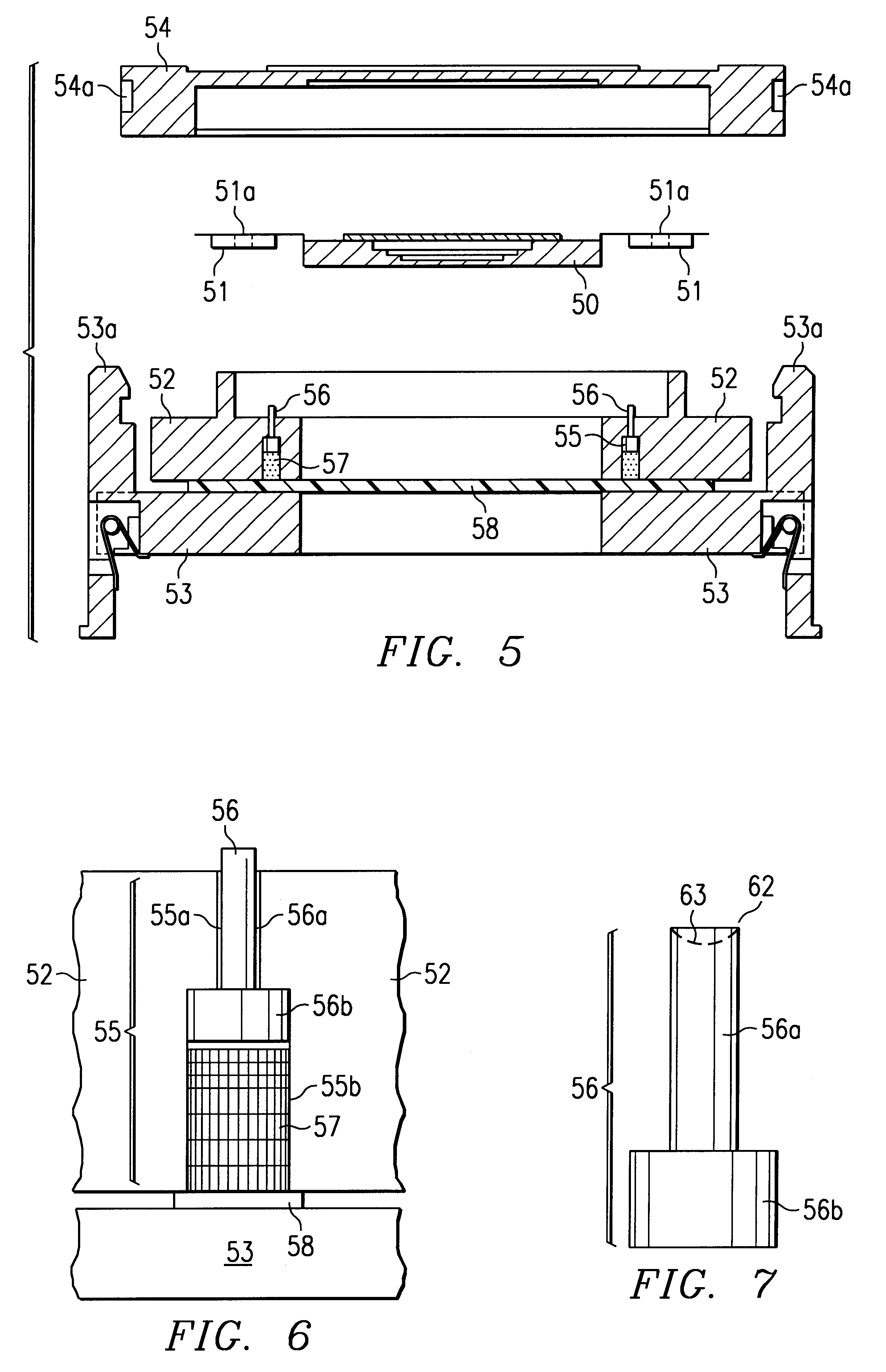
The invention relates to packages of semiconductor devices, specifically of the surface mount and Quad Flat Pack families, that can be used in current semiconductor device production, and to a method of automated testing. The packages have a plurality of insulating tie bars supporting a multitude of leads. The tie bars are designed so that they comprise celectrically conductive vias in a pattern expanding the effective lead pitch for more convenient testing, without introducing unwanted side effects. The full benefit of the expanded lead pitch can be exploited during the electrical testing of the device which utilizes a test apparatus simplified for an automated testing procedure. The base of the apparatus includes a multitude of electrically conductive and mechanically elastic passageways with surface contours adapted for contacting the metallic end connectors of the semiconductor device-to-be-tested, as well as the metallic connector to the tester.

Description

This invention relates generally to the field of integrated circuit packages and more specifically to apparatus and methods for testing fine lead pitch semiconductor packages.BACKGROUND OF THE INVENTIONThe lead count of surface mount semiconductor devices has been increasing for many years, driven by the need for more power and signal input / output. At the same time, there has been a strong push for smaller outline of the device packages, motivated by the requirement to conserve board space in assembly. These trends are conflicting and have resulted in ever smaller pitch of the package leads. Narrower and closely spaced leads, in turn, make mechanical handling more difficult due to weakened strength and tighter proximity; they also result in distortions of electrical testing due to electrical losses and stray effects.Known technology for the electrical testing of surface mount semiconductor devices leaves much to be desired. Most test contactors currently available for high lead coun...

Claims


Application Information

Patent Timeline
IPC IPC(8): G01R1/04G01R1/02
CPCG01R1/0441G01R1/0466G01R1/045
Inventor SETTLE, KIRK F.NOBLE, JR., DON E.
Owner TEXAS INSTR INC
Learn More