Integrated circuit structure including three-dimensional memory array

a technology of integrated circuits and memory arrays, applied in the field of three-dimensional arrays, can solve the problems of significant power consumption, increase the size of dies, and increase the cost of production

Inactive Publication Date: 2002-05-07
SANDISK TECH LLC
View PDF65 Cites 192 Cited by
  • Summary
  • Abstract
  • Description
  • Claims
  • Application Information

AI Technical Summary

Problems solved by technology

While on-chip voltage generator circuits may relieve a user from supplying a second power supply voltage, such circuits frequently require a significant amount of layout area to implement, which may increase die size substantially, and consequently increase costs.
Moreover, such voltage generator circuits also may consume a significant amount of power relative to the remainder of the circuit, and thus increase the current that must be supplied by the user (e.g., by the VDD power supply).
Any increase in power dissipation may also increase the temperature of the die during operation.
In a battery-powered environment, any increase in power consumed by a memory device may have significant implications for battery life, and any additional heat generated may also be difficult to dissipate.
Traditional implementations of on-chip voltage generators, such as charge pumps, may consume an undesirably large amount of die area, particularly relative to a higher bit density memory array.

Method used


Image

  • Integrated circuit structure including three-dimensional memory array
  • Integrated circuit structure including three-dimensional memory array
  • Integrated circuit structure including three-dimensional memory array

Examples


Embodiment Construction

)

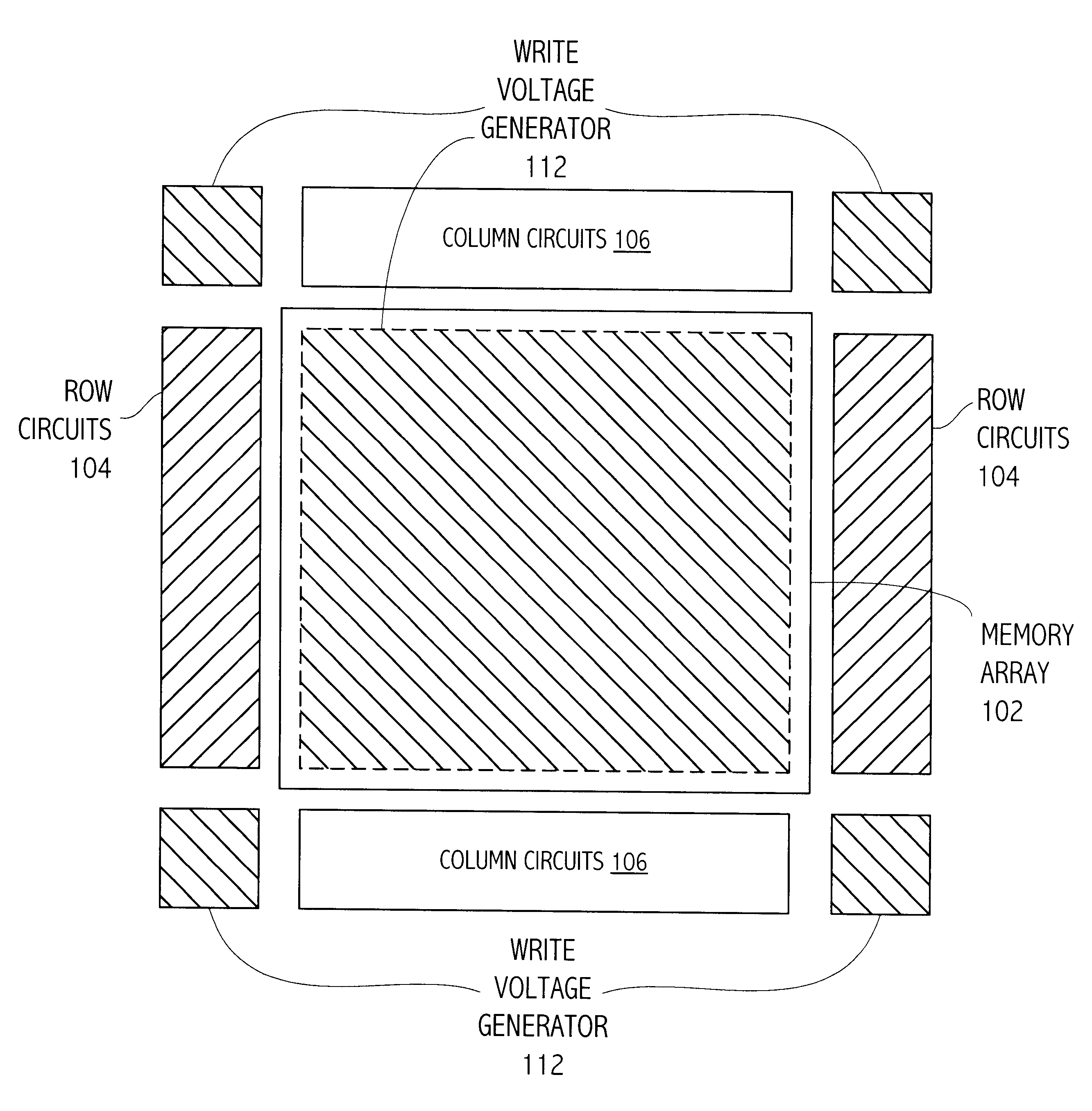
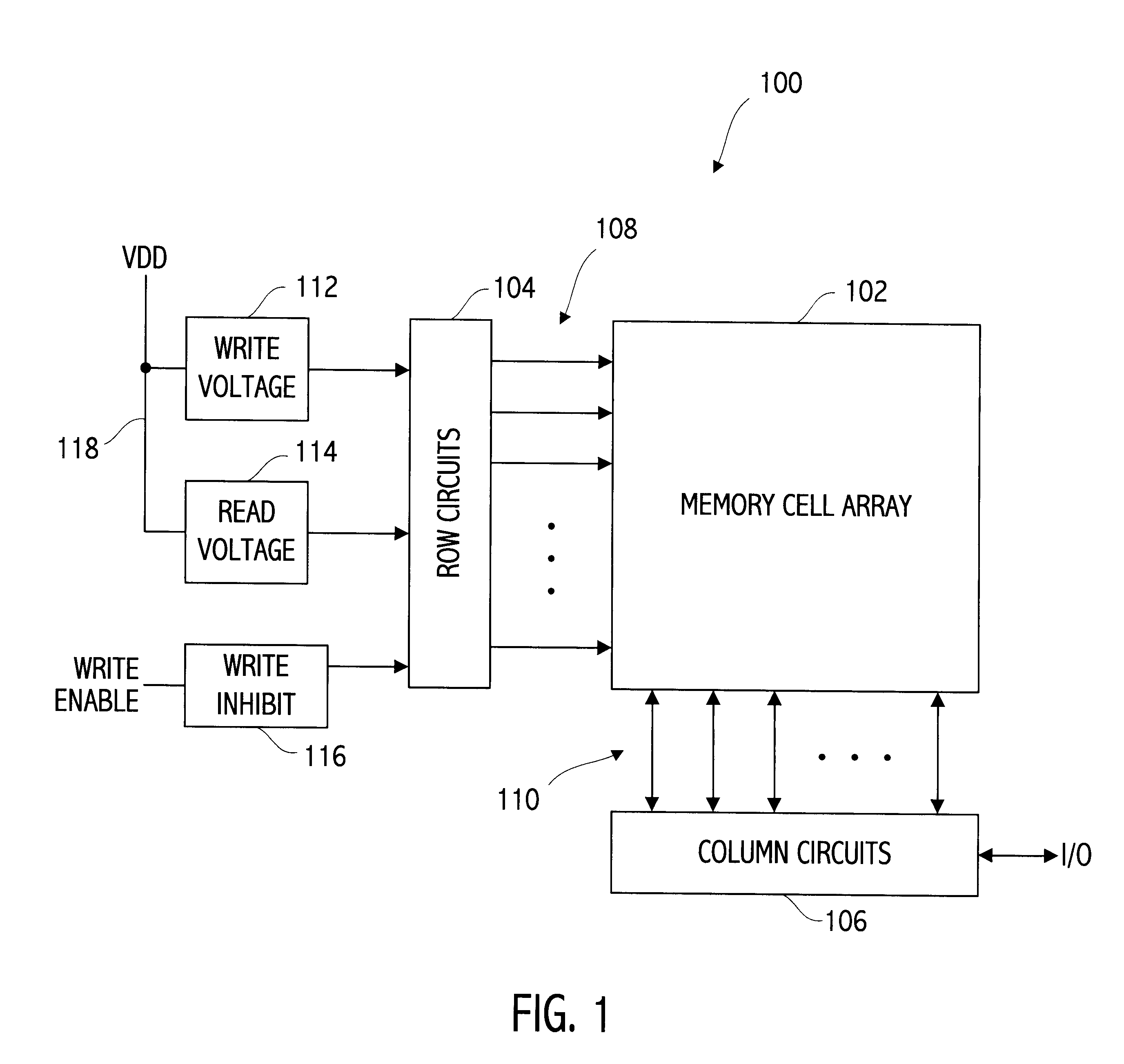
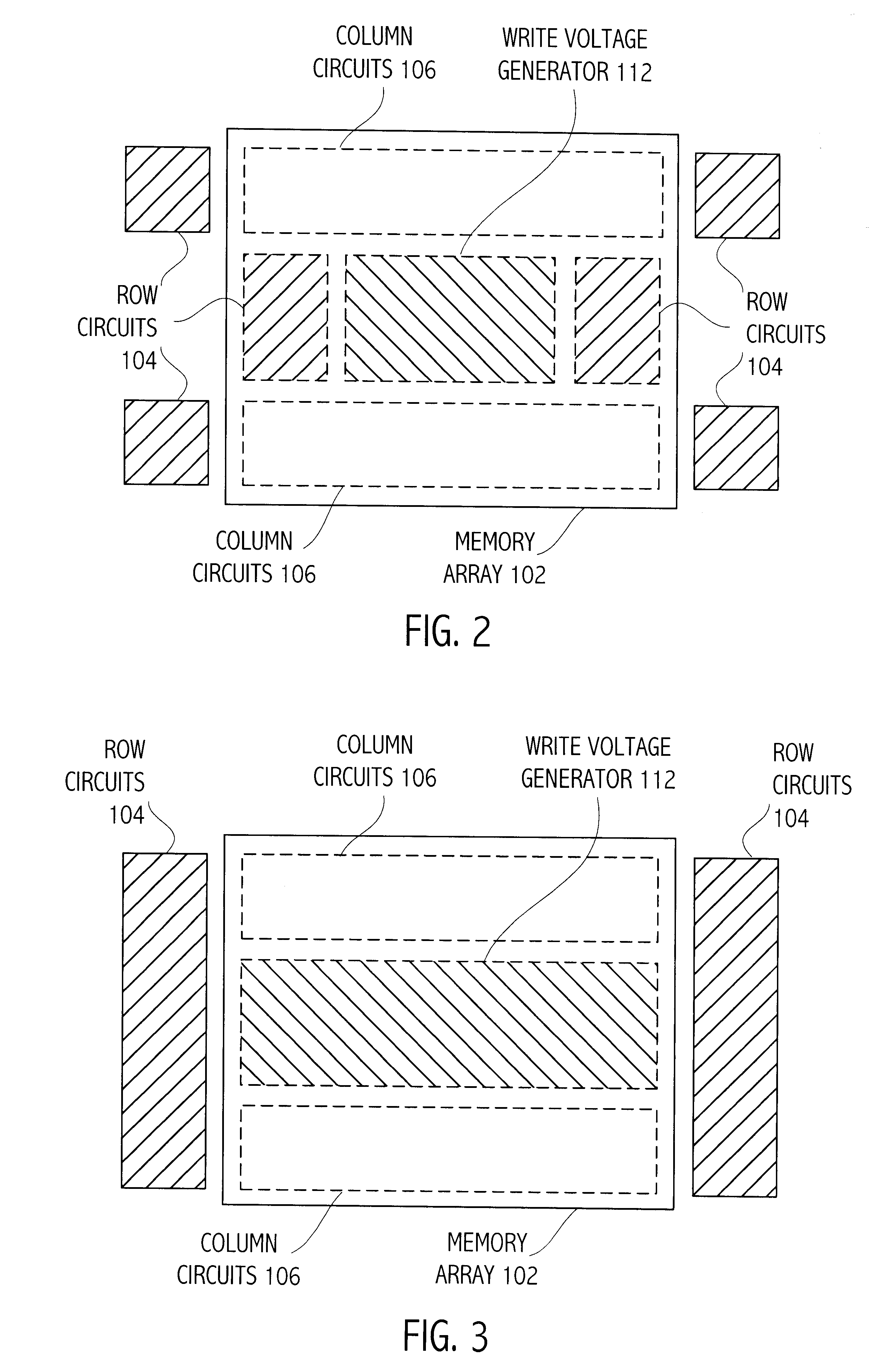
Referring now to FIG. 1, a block diagram is shown of an integrated circuit 100 including a memory array 102, which diagram may be useful to depict several preferred embodiments of the present invention. In one such embodiment, the memory array 102 is preferably a three-dimensional, field-programmable, non-volatile memory array having more than one level of memory cells, and also utilizing a read voltage different in magnitude from a write voltage. Preferred three-dimensional memory arrays are disclosed in commonly-assigned U.S. Pat. No. 6,034,882, entitled "Vertically Stacked Field Programmable Nonvolatile Memory and Method of Fabrication." Another preferred three-dimensional, non-volatile memory array technology is disclosed in co-pending, commonly-assigned U.S. application Ser. No. 09 / 560,626, entitled "Three-Dimensional Memory Array and Method of Fabrication," filed Apr. 28, 2000 and naming as inventor N. Johan Knall, which application is incorporated herein by reference in its ...


PUM


Abstract

An integrated circuit device includes a three-dimensional memory array and array terminal circuitry for providing to selected memory cells of the array a write voltage different from a read voltage. Neither voltage is necessarily equal to a VDD power supply voltage supplied to the integrated circuit. The write voltage, particularly if greater than VDD, may be generated by an on-chip voltage generator, such as a charge pump, which may require an undesirably large amount of die area, particularly relative to a higher bit density three-dimensional memory array formed entirely in layers above a semiconductor substrate. In several preferred embodiments, the area directly beneath a memory array is advantageously utilized to layout at least some of the write voltage generator, thus locating the generator near the selected memory cells during a write operation.

Description

1. Field of the InventionThe present invention relates to semiconductor integrated circuits having memory cell arrays, and particularly to three-dimensional arrays incorporating multiple levels of memory cells.2. Description of the Related ArtSemiconductor memories often use two different voltages to perform the read and write operations. In some memory technologies, particularly nonvolatile memories (i.e., memories having data stored which is not lost or altered when power is removed), the write voltage is often higher than the read voltage, with sufficient margin between the two voltages to ensure that memory cells are not written unintentionally when subjected to the read voltage.Flash memories create a non-volatile state by accelerating electrons across a tunneling dielectric and storing the charge on a floating gate above a field effect transistor. On many earlier-developed devices, this acceleration of charge across the tunneling dielectric frequently required a voltage on the...

Claims


Application Information

Patent Timeline
Patent Type & Authority Patents(United States)
IPC IPC(8): G11C11/56G11C17/14G11C17/16H01L27/102
CPCG11C11/5692G11C17/14G11C17/16H01L27/0203H01L27/1021H01L27/115G11C2213/71H10B69/00
Inventor JOHNSON, MARK G.LEE, THOMAS H.SUBRAMANIAN, VIVEKFARMWALD, PAUL MICHAELCLEEVES, JAMES M.
Owner SANDISK TECH LLC
Why Eureka
Try Eureka