Liquid crystal display with tft array substrate and manufacturing method thereof

a technology of liquid crystal display and array substrate, which is applied in the field of liquid crystal display, can solve the problems of increased parasitic capacity cdp, inability to increase the aperture ratio of the liquid crystal display, and crosstalk, and achieves the effects of low crosstalk, high quality, and hardly increasing parasitic capacity cdp

Inactive Publication Date: 2002-06-11
MITSUBISHI ELECTRIC CORP
View PDF10 Cites 34 Cited by
  • Summary
  • Abstract
  • Description
  • Claims
  • Application Information

AI Technical Summary

Benefits of technology

Accordingly, an object of the present invention is to provide a TFT-LCD (LCD is an abbreviation of liquid crystal display) of high quality in which parasitic capacity Cdp hardly increases and crosstalk is small by arranging a pixel electrode on a source line through a Cs line.
A further object of the invention is to provide a liquid crystal display of high yield.

Problems solved by technology

When the parasitic capacity Cdp becomes large, a problem of crosstalk occurs.
In other words, there arises a problem that, as the crosstalk occurs when decreasing the distance between the pixel electrode 114 and the source line 107, it is necessary to secure a distance exceeding a certain value between the pixel electrode and the source line.
As a result, aperture ratio of the liquid crystal display cannot be increased.
As discussed above, in the pixel structure of the conventional TFT array substrate, there is a problem that when decreasing the distance between the pixel electrode and the source line to improve the aperture ratio, the parasitic capacity Cdp is increased, eventually resulting in occurrence of crosstalk.
It is well known that if the variation is large, there arises a flicker in image plane, and a phenomenon (hereinafter referred to printing) takes place in which when a pattern is continuously displayed for a long time, the same pattern still remains after being switched to the other pattern, which results in deterioration of display quality.
On the other hand, in the liquid crystal display, the light transmitted through the part other than the pixel electrode 205 brings about a disadvantage of deterioration of display quality such as lowering in contrast ratio.
In this respect, as compared with the case of forming a shade film on the array substrate, when shading the leak light by the shade film arranged on the counter substrate, alignment accuracy of the counter substrate and the array substrate is lower than the pattern accuracy of the array substrate, resulting in a large shading region.
When occurs such a defect of short circuit, any scanning signal is not supplied normally, which is visually recognized as defective line.
However, in the event that such a defect of short circuit takes place under the source line 201, a problem exists in that when interrupting the short circuit portion, the source line 201 is also interrupted and visually recognized as defective source line, making it impossible to repair the defect.

Method used


Image

  • Liquid crystal display with tft array substrate and manufacturing method thereof
  • Liquid crystal display with tft array substrate and manufacturing method thereof
  • Liquid crystal display with tft array substrate and manufacturing method thereof

Examples


example 1

of the invention is hereinafter described.

The invention is characterized by its structure in the pixel section of TFT array, and a difference from the prior art is hereinafter described with reference to the drawings.

In a liquid crystal display according to the invention, the Cs lines are formed on the upper layer of the source lines to cover them, and the pixel electrodes are further arranged and formed on the upper layer thereof in such a manner as to overlap partially.

Basic construction of the liquid crystal display is same as that according to the prior art.

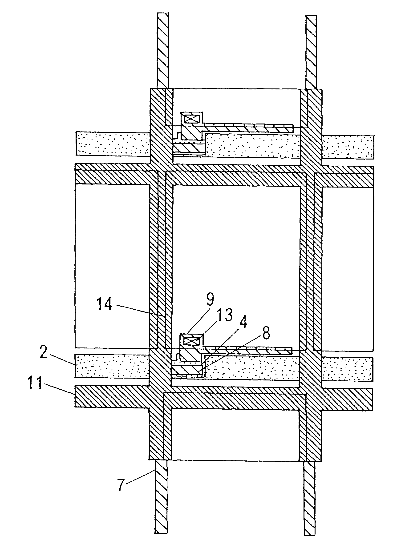
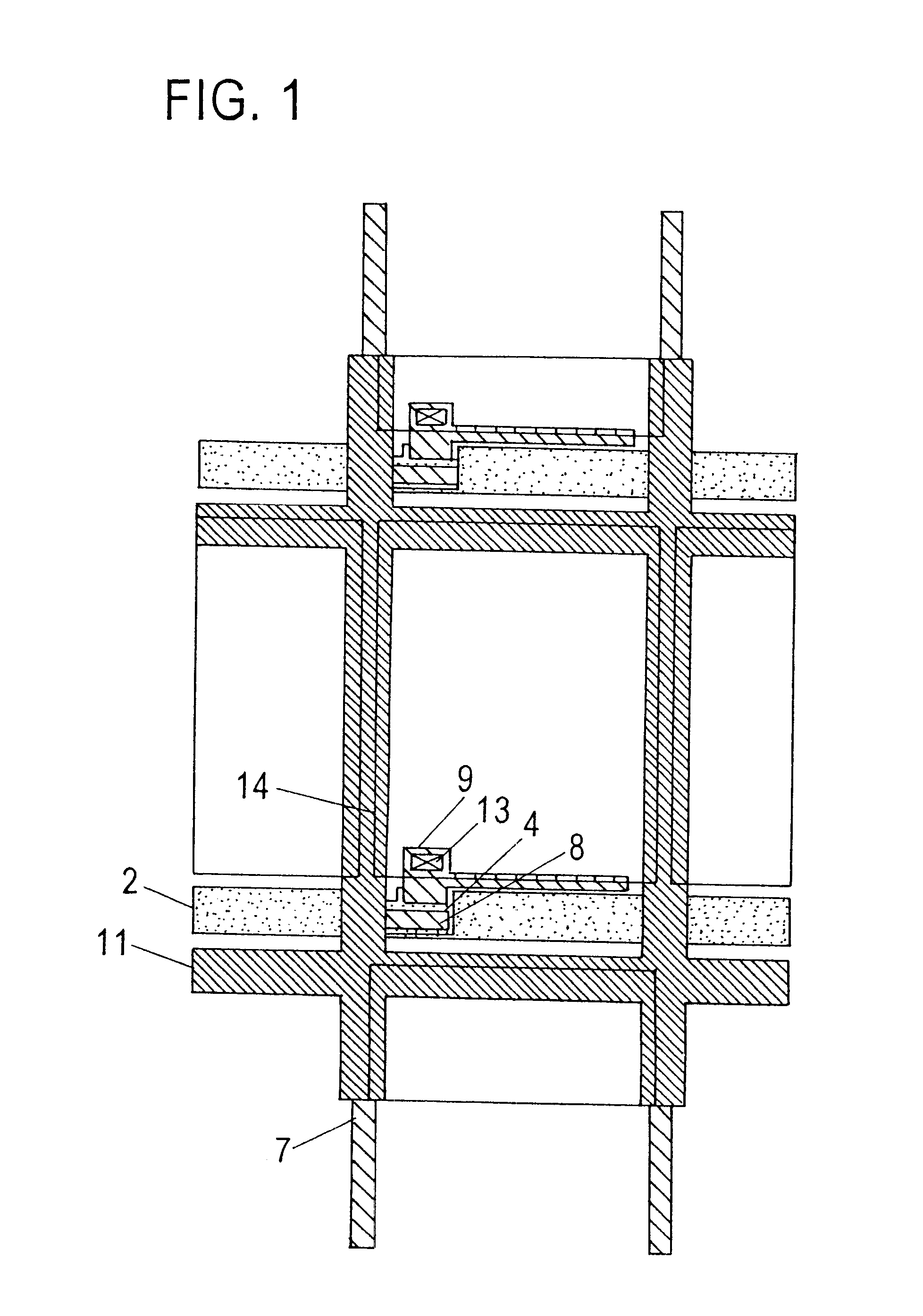
FIG. 1 is a plan view of a liquid crystal display according to example 1 of the invention. In the drawing, reference numeral 2 indicates a gate line, numeral 4 indicates a semiconductor thin film forming a TFT, numeral 7 is a source line, numeral 8 is a source electrode, numeral 9 is a drain electrode, numeral 11 is a Cs line, numeral 14 is a pixel electrode, and numeral 13 is a contact for electrically connecting the pixel e...

example 2

Example 2 of the invention is hereinafter described.

The manufacturing method of the pixel section according to this example 2 is same as that shown in example 1, as far as the manufacturing steps before forming a Cs line 11a are concerned.

As shown in FIG. 9, the Cs line 11a does not form a line section parallel to the gate line 2 in the pixel, but is arranged and formed above the source line 7 and an adjacent source line 7 through the source insulating film by overlapping a part of a pixel electrode 14a on the adjacent gate line 2. The Cs line 11a is not formed into a ring being different from example 1, but is arranged along the longitudinal direction (shorter direction than lateral direction) of liquid crystal panel. As a result, the line resistance can be restrained to be small as compared with the arrangement in lateral direction.

By forming the pixel electrode 14a shown in FIG. 9, the distance between the source line 7 and the pixel electrode 14a can be reduced thereby improving...

example 3

Example 3 of the invention is hereinafter described.

FIG. 10 is a plan view showing a pixel of the liquid crystal display according to example 3 of the invention. The pixel shown in FIG. 10 is arranged forming a matrix and forms a display section.

In the drawing, reference numeral 201 indicates a source line, numeral 202 indicates a gate line arranged crossing over the source line 201, and numeral 203 is a Cs line forming a storage capacitance which is arranged along the gate line 202 and formed in the same manufacturing step as that of the gate line 202.

Numeral 204 is a semiconductor layer forming a channel of TFT, and numeral 205 is a pixel electrode forming a display section and is formed in a region defined by the source line 201 and the gate line 202. Numeral 206 is a drain electrode of TFT which is connected to the pixel electrode 205. The semiconductor 204, the source line 201, the gate line 202 and the drain electrode 206 form a TFT.

FIG. 11 is a plan view showing an interrupti...


PUM

PropertyMeasurementUnit
voltageaaaaaaaaaa
voltageaaaaaaaaaa
storage capacitanceaaaaaaaaaa

Abstract

Parasitic capacity between Cs lines and source lines forming a pixel section is reduced, whereby characteristic resistant to crosstalk is achieved, aperture ratio is increased, and brightness of LCD is increased. The Cs lines are arranged on the source lines in such a manner as to cover the source lines, and pixel electrodes are arranged and formed on the Cs lines in such a manner as to partially overlap. By forming a structure in which the source lines, the Cs lines and the pixel electrodes are laminated in order, parasitic capacity between the Cs lines and the source lines forming a pixel section can be reduced, and crosstalk can be minimized. As a distance between the source lines and the pixel electrodes can be reduced from the viewpoint of a plan view, aperture ratio can be improved.

Description

1. Field of the InventionThe present invention relates to a liquid crystal display provided with a thin film transistor array substrate for use in matrix type display and to a manufacturing method thereof.2. Description of the Prior ArtGenerally, a matrix type display comprises a thin film transistor array substrate (hereinafter referred to as TFT array substrate) on which a thin film transistor (hereinafter referred to as TFT) is formed, and a counter substrate on which color filter, black matrix, etc. are formed. A display material such as liquid crystal is held between the mentioned two substrates, and in which a voltage is selectively applied to the display material.In the TFT array substrate, as shown in the equivalent circuit of FIG. 14, pixels are arranged forming a matrix.In FIG. 14, reference numerals G1, G2, G3 indicate scanning signal lines (hereinafter referred to as gate lines), and numerals S1, S2, S3 indicate image signal lines (hereinafter referred to as source lines...

Claims


Application Information

Patent Timeline
Patent Type & Authority Patents(United States)
IPC IPC(8): G02F1/13G02F1/1362G02F1/1345G02F1/136
CPCG02F1/136213G02F1/1345G02F1/136
Inventor NAKAYAMA, AKIONUMANO, YOSHINORI
Owner MITSUBISHI ELECTRIC CORP
Why Eureka
Try Eureka