Method and apparatus for forming insitu boron doped polycrystalline and amorphous silicon films

a polycrystalline and polycrystalline silicon film, insitu technology, applied in the direction of coatings, chemical vapor deposition coatings, metallic material coating processes, etc., can solve the problems of low deposition rate, difficult to obtain uniform thickness film and dopant concentration from wafer to wafer and batch to batch

Inactive Publication Date: 2002-06-25
APPLIED MATERIALS INC
View PDF6 Cites 21 Cited by
  • Summary
  • Abstract
  • Description
  • Claims
  • Application Information

AI Technical Summary

Problems solved by technology

Although LPCVD processes can form high quality films, their low deposition rates necessitate the processing of multiple wafers (i.e. up to 100) at one time in a batch type reaction vessel.
A problem with processing a plurality of wafers in a single machine at a single time is that it is difficult to obtain uniform thickness film and dopant concentration from wafer to wafer and from batch to batch.

Method used


Image

  • Method and apparatus for forming insitu boron doped polycrystalline and amorphous silicon films
  • Method and apparatus for forming insitu boron doped polycrystalline and amorphous silicon films
  • Method and apparatus for forming insitu boron doped polycrystalline and amorphous silicon films

Examples


Embodiment Construction

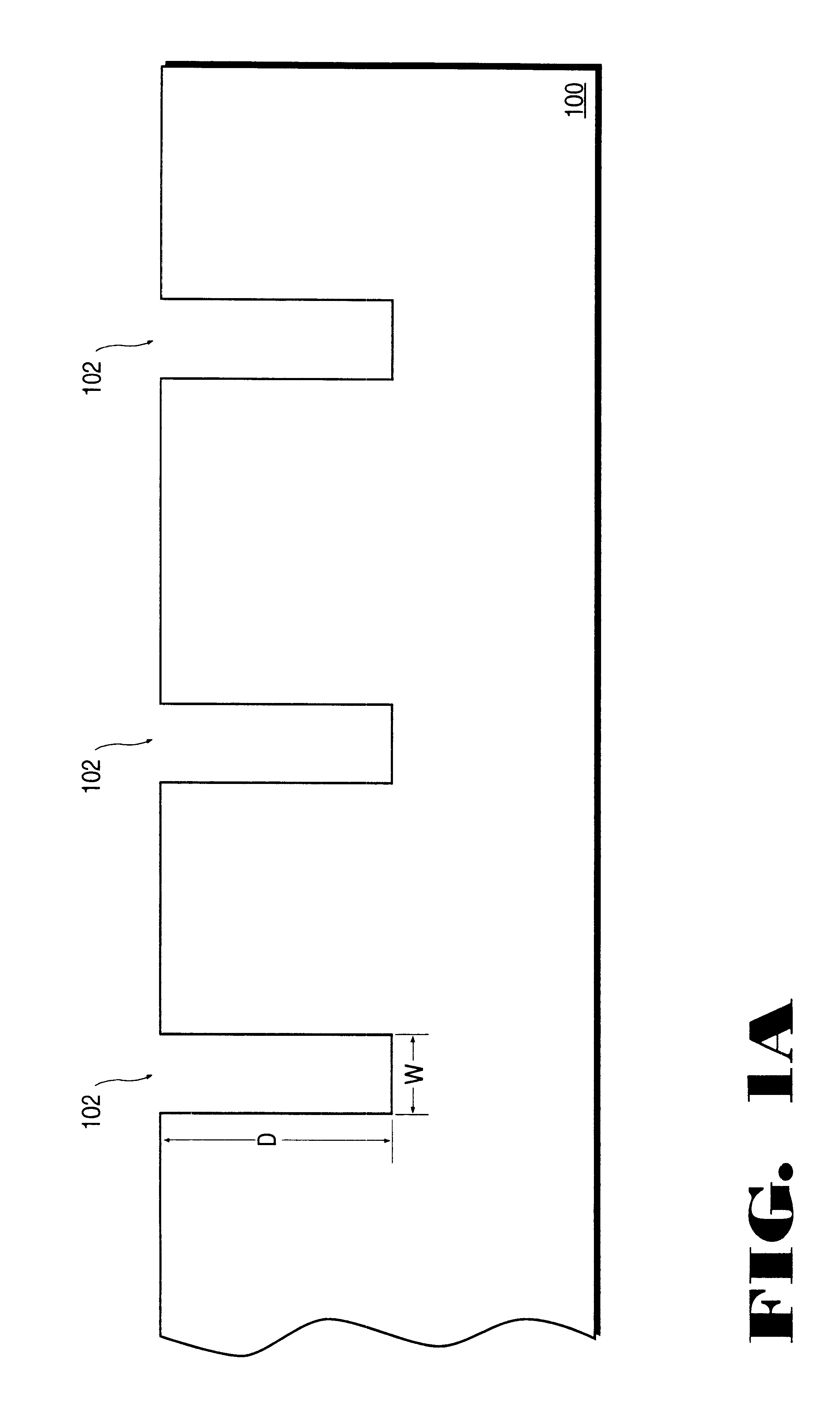
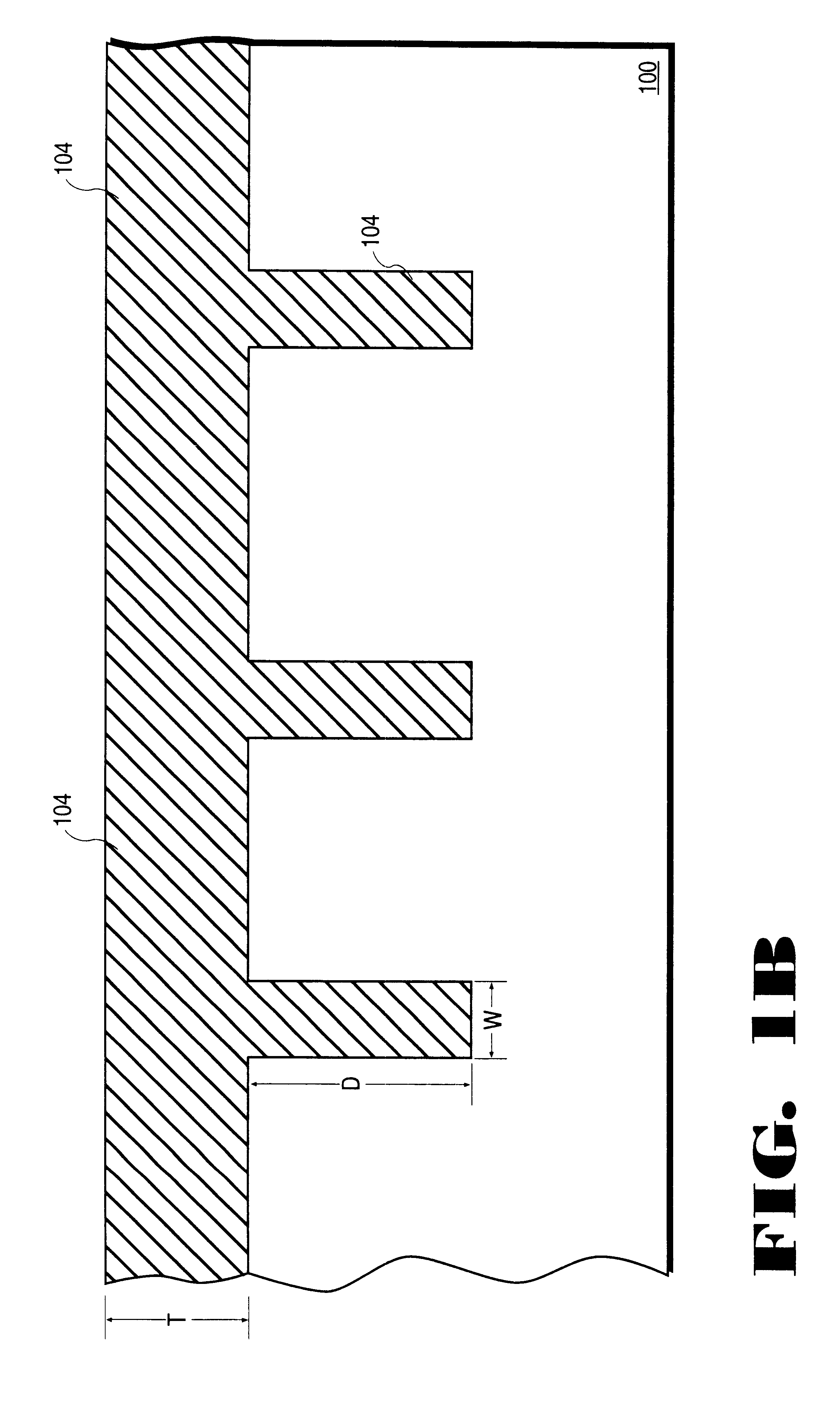
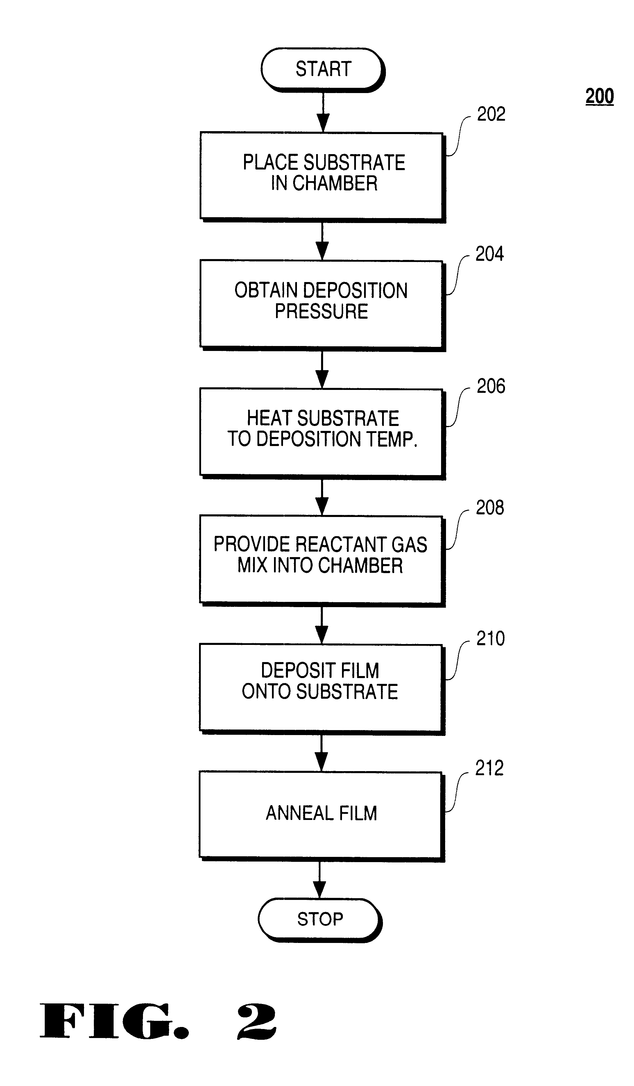
The present invention describes a novel method and apparatus for depositing an insitu boron doped polycrystalline or amorphous silicon film. In the following description, numerous specific details are set forth such as specific process parameters and implementation in order to provide a thorough understanding of the present invention. It will be obvious, however, to one skilled in the art, that the present invention may be practiced without the specific details. In other instances, well known chemical vapor deposition (CVD) equipment and semiconductor methodology have not been described in particular detail in order to not necessarily obscure the present invention.

The present invention describes a method and apparatus for depositing an insitu boron doped polycrystalline or amorphous silicon film at a high deposition rate and with good step coverage. According to the present invention, a substrate (or wafer) is placed into a deposition chamber of a thermal chemical vapor deposition (...


PUM

PropertyMeasurementUnit
pressureaaaaaaaaaa
temperatureaaaaaaaaaa
residence timeaaaaaaaaaa

Abstract

A method and apparatus for depositing a boron insitu doped amorphous or polycrystalline silicon film on a substrate. According to the present invention, a substrate is placed into deposition chamber. A reactant gas mix comprising a silicon source gas, boron source gas, and a carrier gas is fed into the deposition chamber. The carrier gas is fed into the deposition chamber at a rate so that the residence of the carrier gas in the deposition chamber is less then or equal to 3 seconds or alternatively has a velocity of at least 4 inches / sec. In another embodiment of forming a boron doped amorphous for polycrystalline silicon film a substrate is placed into a deposition chamber. The substrate is heated to a deposition temperature between 580-750° C. and the chamber pressure reduced to a deposition pressure of less than or equal to 50 torr. A silicon source gas is fed into the deposition at a rate to provide a silicon source gas partial pressure of between 1-5 torr. Additionally, a boron source gas is fed into the deposition chamber at a rate to provide a boron gas partial pressure of between 0.005-0.05 torr.

Description

1. Field of the InventionThe present invention relates to the field of thin film formation, and more particularly to a method and apparatus for depositing an insitu boron doped amorphous or polycrystalline silicon film.2. Discussion of Related ArtPolycrystalline silicon (polysilicon) and amorphous silicon thin films are used throughout the many semiconductor integrated circuit manufacturing processes. These films are used, for example, in the fabrication of gate electrodes, stack or trench capacitors, emitters, contacts, fuses, and antifuses. As device dimensions decrease to below 0.25 microns in order to increase packing density, aspect ratios (aspect ratio=depth / width) of holes, vias, and trenches in the integrated circuit are also increasing. In order to fill high aspect ratio openings (aspect ratios .gtoreq. to 2.5), deposition processes which are capable of good step coverage (step coverage %=film thickness on a step surface / film thickness on a flat surface.times.100%) are requ...

Claims


Application Information

Patent Timeline
Patent Type & Authority Patents(United States)
IPC IPC(8): C23C16/22C23C16/24H01L21/02H01L21/205C23C16/44C23C16/455H01L21/285
CPCC23C16/24C23C16/45502H01L21/02381H01L21/02661H01L21/02532H01L21/02579H01L21/0262H01L21/02395
Inventor WANG, SHULIN
Owner APPLIED MATERIALS INC
Why Eureka
Try Eureka