

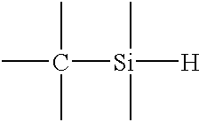
Formation of a liquid-like silica layer by reaction of an organosilicon compound and a hydroxyl forming compound
a technology of organosilicon and hydroxyl group, which is applied in the direction of plasma technique, semiconductor/solid-state device details, coatings, etc., can solve the problems of difficult to feed exact amounts of hydrogen peroxide and silane within the reaction chamber, and the available methods for forming silicon oxide that contains hydroxyl groups do not provide uniform dielectric layers
- Summary
- Abstract
- Description
- Claims
- Application Information
AI Technical Summary
Problems solved by technology
Method used
Image

Examples
examples
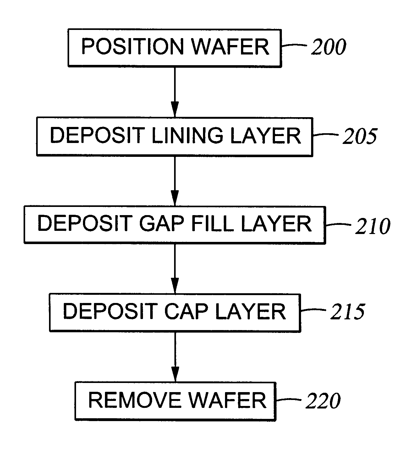
The following examples illustrate reaction of an organosilicon compound and hydroxyl forming compounds to deposit dielectric layers having low dielectric constants. The examples refer to a chemical vapor deposition chamber, and in particular, a "CENTURA DxZ" system which includes a solid-state RF matching unit with a two-piece quartz process kit, both fabricated and sold by Applied Materials, Inc., Santa Clara, Calif.
Peroxide Source (Hypothetical)
An oxidized trimethylsilane film is deposited at a chamber pressure of 3.0 Torr and a substrate temperature of 0.degree. C. from reactive gases which are flowed into the reactor as follows:
The substrate is positioned from 200-1000 mils from the gas distribution showerhead, preferably 600 mils, and deposition occurs to a depth from about 1000 .ANG. to 2 .mu.m. The film is then cured at a temperature of 400.degree. C. for about 30 to about 120 minutes. The oxidized trimethylsilane material is estimated to have a dielectric constant less than ...
PUM
| Property | Measurement | Unit |
|---|---|---|
| Temperature | aaaaa | aaaaa |
| Temperature | aaaaa | aaaaa |
| Fraction | aaaaa | aaaaa |
Abstract
Description
Claims
Application Information