Programmable timing circuit for testing the cycle time of functional circuits on an integrated circuit chip

a technology of integrated circuits and timing circuits, which is applied in the direction of pulse manipulation, pulse technique, instruments, etc., can solve the problems of psros no longer being accessible for re-verification, difficulty in accumulation and analysis of data, and a bit lower chip yield

Inactive Publication Date: 2002-07-02
IBM CORP
View PDF23 Cites 25 Cited by
  • Summary
  • Abstract
  • Description
  • Claims
  • Application Information

AI Technical Summary

Benefits of technology

It is an advantage of the invention that an on-chip test circuit is provided for facilitating HBCT activities.It is a further advantage of the invention that an improved method for HBCT analysis in the determination of sort points is provided.It is a further advantage of the invention that there is provided an improved capability for testing functional circuits on integrated circuit chips following dicing and mounting of the chips to substrates.It is a further advantage of the invention that there is provided a method and apparatus for gathering additional data in a more efficient manner than heretofore possible for HBCT analysis, as well as providing a "built-in" tool for is measuring circuit performance without the need of additional test equipment.It is a further advantage of the invention that there is provided a functional circuit testing capability not requiring test equipment external to the chip containing said circuit.It is a further advantage of the invention that there is provided a programmable configuration of delay on data tapped directly from a functional circuit on an integrated circuit chip.It is a further advantage of the invention that there is provided an apparatus and method for circuit timing measurements under dynamic conditions which allow measurement of the actual path length, particularly if the circuit being measured is not the longest path of the chip design.It is a further advantage of the invention that there is provided an apparatus and method for circuit timing is measurements on functional logic paths having desired characteristics for evaluating chip fabrication process variations which might affect circuit performance.It is a further advantage of the invention that there is provided a functional circuit timing measurement circuit which taps directly off of a selected functional path, without adding logic to a possible critical path.It is a further advantage of the invention that there is provided an apparatus and method for ready detection of failure of an object path as its clock cycle is gradually shortened.It is a further advantage of the invention that there is provided a capability to test any functional logic path, not just logic associated with buffers.

Problems solved by technology

Circuit speeds, i.e., the speed at which logic devices can switch combined with signal transmission rate from device to device, are not identical in all parts of the wafer (or from wafer to wafer) because of uncontrollable inconsistencies in the manufacturing process.
After the chips are packaged (mounted on module substrates), PSROs may no longer be accessible for re-verification, depending on the design.
It is becoming common practice to include HBCT analysis in the determination of sort points since sole reliance on mathematical models based on technology parameters tends towards the conservative resulting in somewhat lower chip yields.
With current HBCT methodology, the accumulation and analysis of data is difficult and time consuming.
It often happens that paths identified as longest by the software timing tools are not necessarily the longest in the actual hardware, if for no other reason than because of "disturb" effects of other circuits which are not factored into the timing calculations.
Long paths that are identified using software timing tools are often very difficult to activate in the actual hardware to allow measurement of the actual path length, particularly if it is not the longest path of the design.
On the other hand, it may require weeks of analysis, depending on the nature of the failure, and then it may only be an educated guess.
With current HBCT techniques it is very difficult to single out a path having the specific characteristics needed for this type of analysis, and be able to make measurements under dynamic conditions.
Once the chips are mounted on module substrates (chip carriers), these particular PSROs outputs may no longer be accessible for subsequent measurements, i.e., no connection is made between chip I / O pad and a module pin so as to minimize the number of module pins, module size, and thereby cost.
Using this method it is very difficult to collect data on other than a few of the longest paths because of limited success in masking or ignoring these errors to measure slightly shorter paths.
Having more than one valid part number for the same physical part creates an exposure to having mixed stock in card and system manufacturing, which, in turn, can lead to highly intermittent errors and very expensive resolutions.

Method used


Image

  • Programmable timing circuit for testing the cycle time of functional circuits on an integrated circuit chip
  • Programmable timing circuit for testing the cycle time of functional circuits on an integrated circuit chip
  • Programmable timing circuit for testing the cycle time of functional circuits on an integrated circuit chip

Examples


Embodiment Construction

It will be appreciated that, although specific embodiments of the invention have been described herein for purposes of illustration, various modifications may be made without departing from the spirit and scope of the invention. In particular, it is within the scope of the invention to provide a memory device, such as a transmission medium, magnetic or optical tape or disc, or the like, for storing signals for controlling the operation of a computer on a chip according to the method of the invention and / or to structure its components in accordance with the apparatus of the invention.

Accordingly, the scope of protection of this invention is limited only by the following claims and their equivalents.


PUM


Abstract

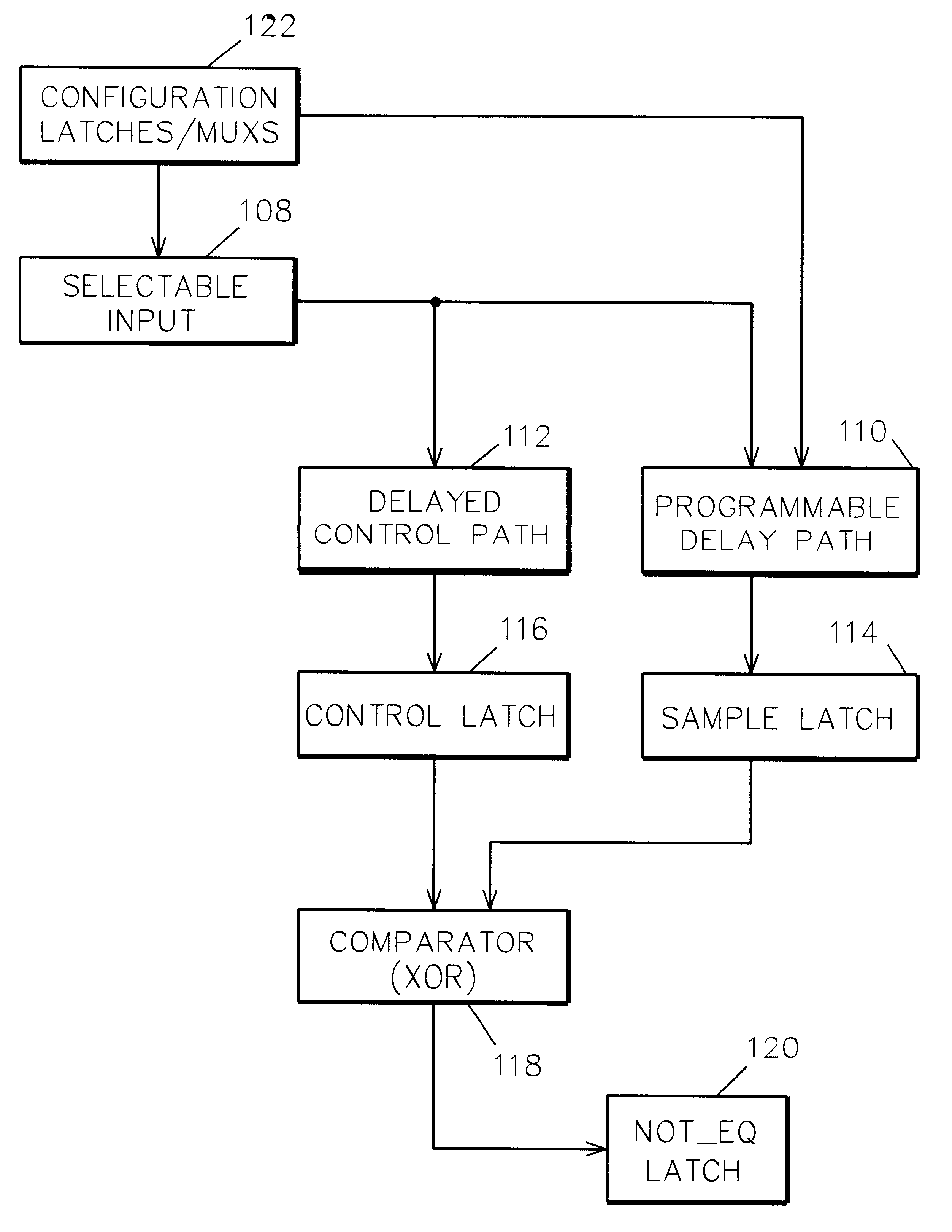
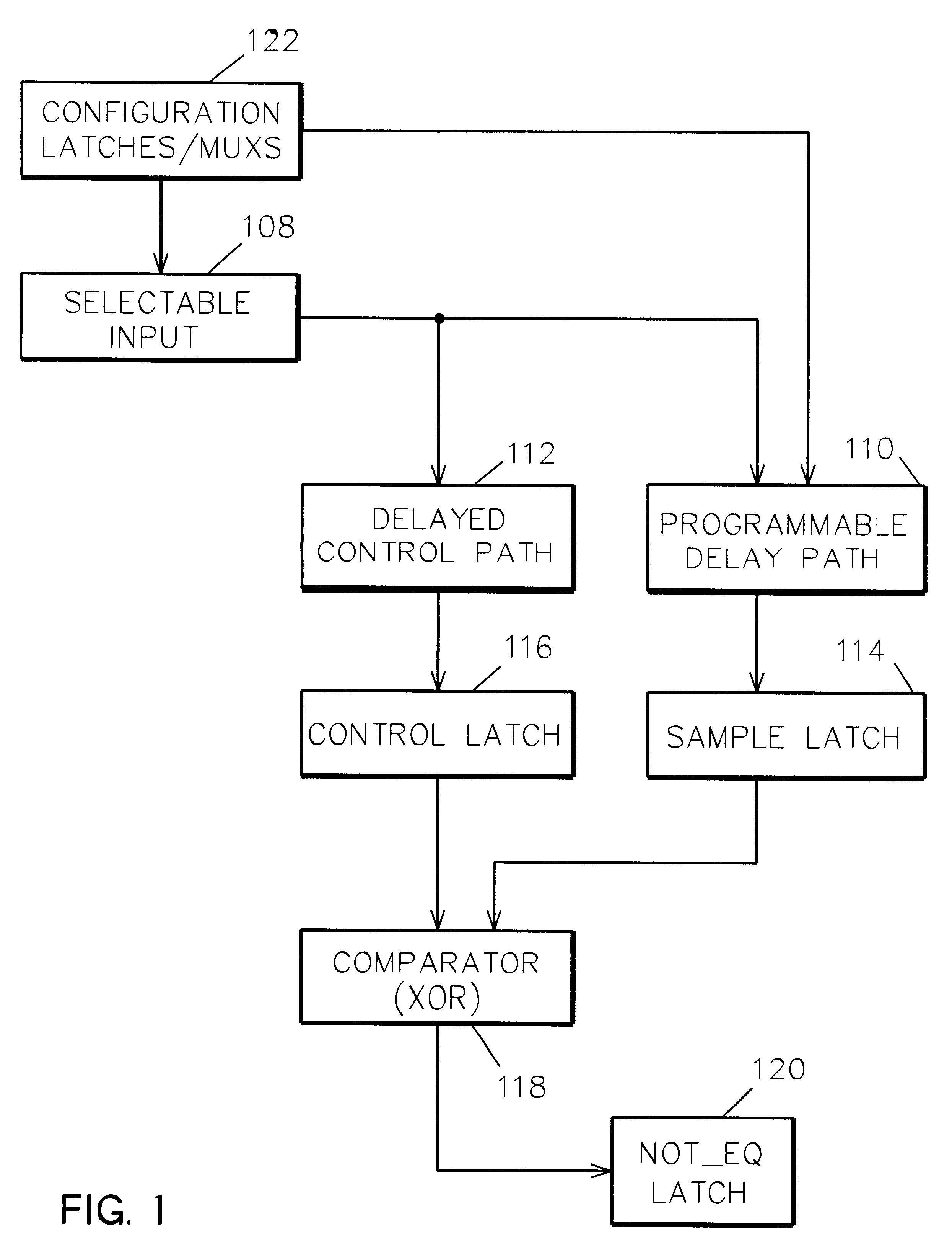
A programmable timing circuit on an integrated circuit chip for testing the cycle time of functional circuits on the chip. The timing circuit includes a selectable input having at least two sources, one of which is a toggle circuit; a minimally delayed control path including a control latch; a programmable delay path in parallel with the control path and including a sample latch; and a comparator for comparing the state of the control latch and sample latches to provide a signal indicative of the delay path being longer than the control path. A plurality of configuration latches and multiplexers are provided for selecting the input source and routing an input signal through specific delay blocks to control the amount of delay in the delay path.

Description

1. Technical Field of the InventionThis invention relates to an apparatus and method for testing the cycle time of functional circuits. More specifically, it relates to an on-chip programmable timing circuit for determining the relative performance of functional circuits and to verify chip circuit performance.2. Background ArtCircuit speeds, i.e., the speed at which logic devices can switch combined with signal transmission rate from device to device, are not identical in all parts of the wafer (or from wafer to wafer) because of uncontrollable inconsistencies in the manufacturing process.A common method for determining the performance of circuitry on an ASIC chip, after fabrication of the wafer, is through the use of Performance Scan-Ring Oscillators (PSROs). A PSRO circuit is essentially a free-running ring of memory elements passing a pulse (a la a bucket-brigade) the output of which can be measured at a reserved chip output pin. Free-running in this case implies a circuit that i...

Claims


Application Information

Patent Timeline
Patent Type & Authority Patents(United States)
IPC IPC(8): G01R31/3193G01R31/28G06F1/02G06F1/025G01R31/30
CPCG01R31/31937G06F1/025G01R31/3016
Inventor BISHOP, JAMES W.FAX, GEORGE A.ISEMINGER, ROBERT G.
Owner IBM CORP
Why Eureka
Try Eureka