Sense amplifier and method for sensing signals in a silicon-on-insulator integrated circuit

a silicon-on-insulator integrated circuit and signal sensing technology, applied in the field of digital integrated circuits, can solve the problems of reducing the switching speed of transistors formed in non-insulating technologies, and affecting the operation of sense amplifiers

Inactive Publication Date: 2002-08-13
IBM CORP
View PDF4 Cites 80 Cited by
  • Summary
  • Abstract
  • Description
  • Claims
  • Application Information

AI Technical Summary

Benefits of technology

will be apparent from the

Problems solved by technology

In non-insulated technologies, the substrate is biased to a power supply rail, raising the capacitive loading on the transistor terminals and thus reducing the switching speed of the transistors formed in non-insulated technologies.
The bitlines are the outputs of the storage array and the access delay of the memory may be limited by the capacitance of the bitline.
This speed limitation is also dependent on the power supply voltage within the storage array, since for reduced power supply voltage, the voltage differential is proportionately reduced at time of measur

Method used


Image

  • Sense amplifier and method for sensing signals in a silicon-on-insulator integrated circuit
  • Sense amplifier and method for sensing signals in a silicon-on-insulator integrated circuit
  • Sense amplifier and method for sensing signals in a silicon-on-insulator integrated circuit

Examples


Embodiment Construction

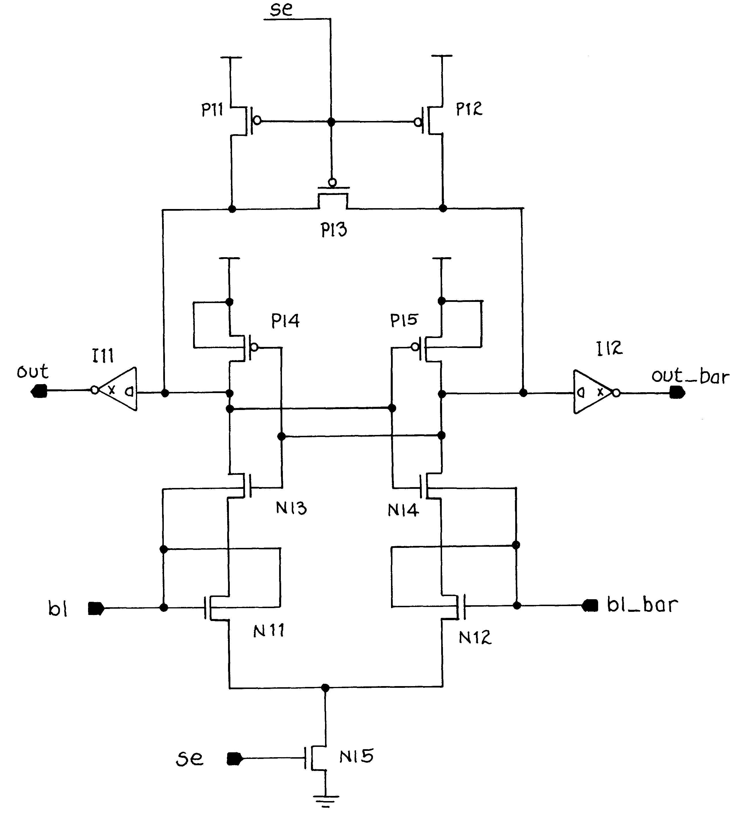
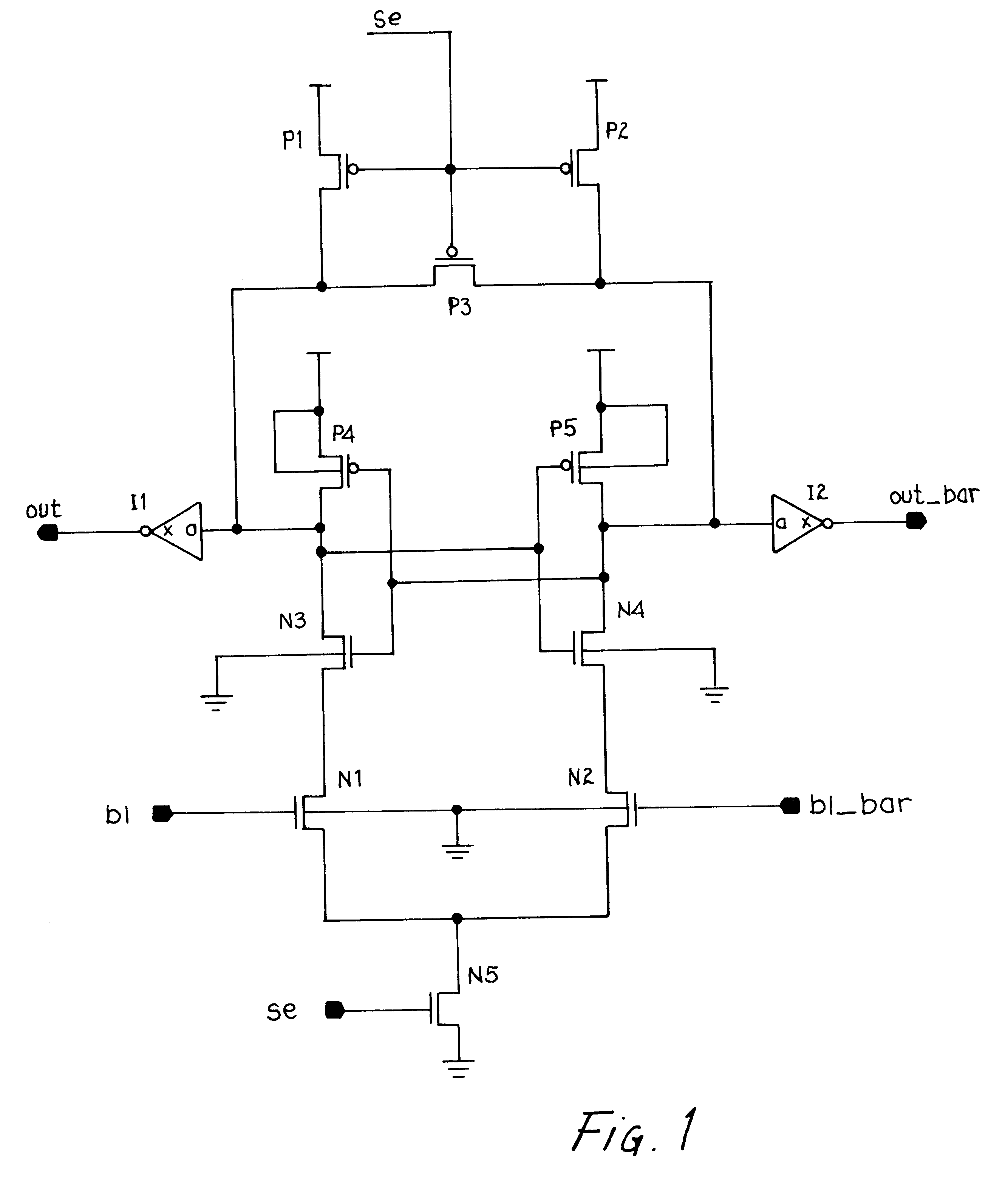
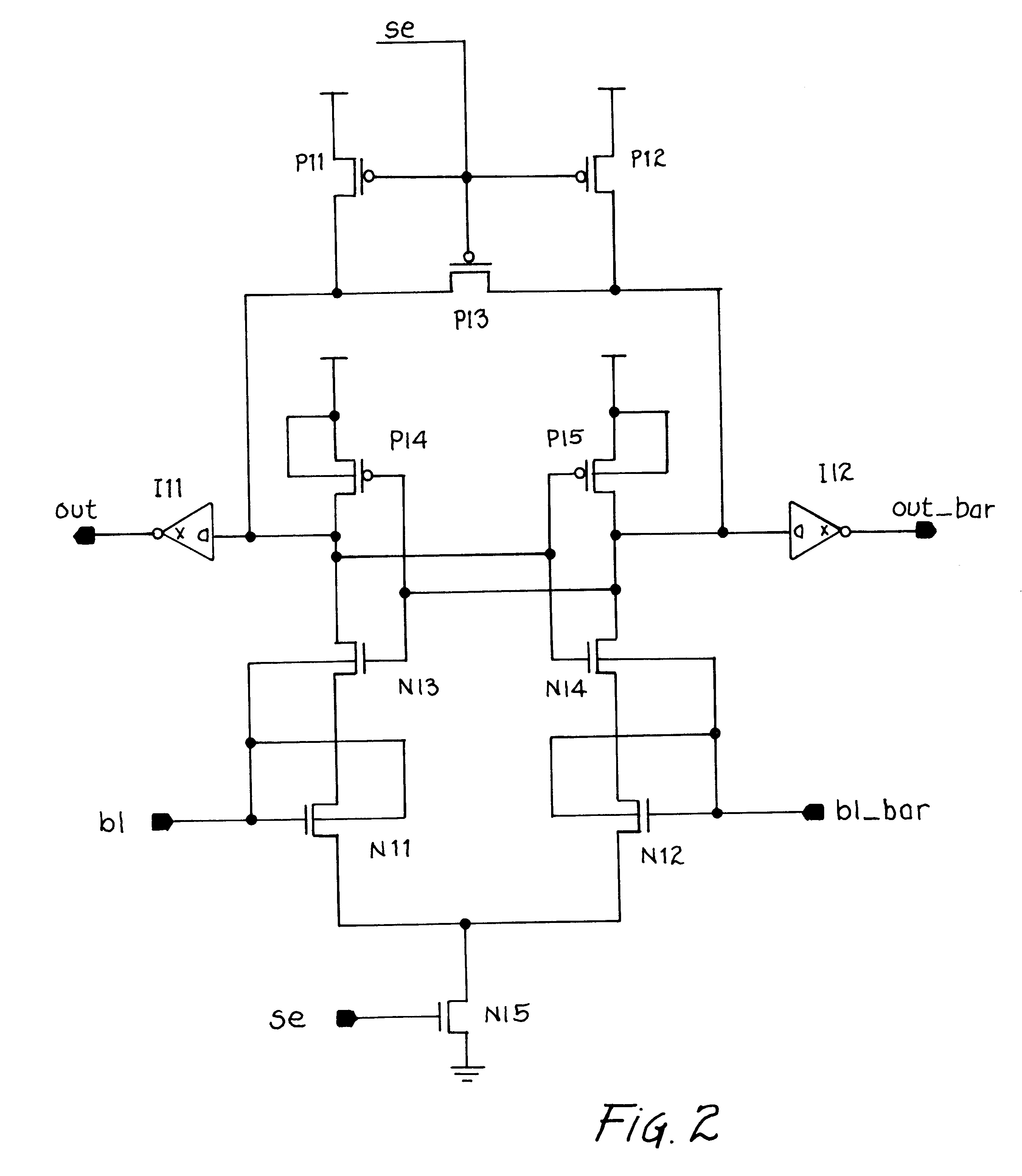
Referring to FIG. 1, a dynamic logic circuit embodying a sense amplifier having a buffered input stage is depicted. Latch transistors N3 and N4 form a cross-coupled pair that provide complementary outputs to output inverters I1 and I2. Latch transistors P4 and P5 are of complementary type to latch transistors N3 and N4, providing a complementary cross-coupled stage that holds a state of the sense amplifier. In the circuits described in the above-incorporated patent application "METHOD AND APPARATUS FOR FAST SOI BASED AMPLIFIER", the inputs to the sense amplifier are applied directly to the inputs of the output inverters, requiring that inputs to the dynamic logic circuit be capable of driving the circuit loads associated with all of the components that are coupled to the input of an output inverter. In the circuit of FIG. 1 (as well as in the embodiments of the present invention), input transistors N1 and N2 are provided to isolate the input signals which are generally the outputs o...


PUM


Abstract

An improved sense amplifier ad method for sensing signals in a silicon-on-insulator (SOI) integrated circuit improve the performance of semiconductor memories and other circuits implemented in SOI technology. The bodies of amplifier transistors within the sense amplifier and bodies of input transistors to the sense amplifier are coupled to corresponding input signals, eliminating the history dependance that would result from unconnected bodies, while achieving faster switching times due to a dynamically produced difference in threshold voltage of the input transistors and amplifier transistors. The switching time is improved over circuits using input transistors and amplifier transistors having statically biased bodies.

Description

1. Technical FieldThe present invention relates to digital integrated circuits, and more particularly to dynamic logic circuits implemented in Silicon-On-Insulator (SOI) technology wherein differential signals are detected.2. Description of the Related ArtDynamic logic circuits are frequently used in integrated circuits, particularly in very large scale integrated circuits (VLSI). Dynamic logic circuits are widely used in semiconductor memories, microprocessors and large logic arrays. Recently, Silicon-On-Insulator (SOI) technology has been used to implement dynamic circuits within semiconductor memories and microprocessors. SOI integrated circuits provide shorter delays and lower power dissipation due to reduced substrate capacitance. SOI channel material is formed within a "trench" above an oxide insulating layer, reducing resistive leakage to the substrate and capacitive loading by the substrate. The "body" of an SOI transistor is the channel material to which the source and drai...

Claims


Application Information

Patent Timeline
IPC IPC(8): G11C7/06H03K3/00H03K3/012H03K3/356
CPCG11C7/065H03K3/012H03K3/356139
Inventor LEE, MICHAEL JU HYEOK
Owner IBM CORP
Why Eureka
Try Eureka