Liquid crystal display in which at least one pixel includes both a transmissive region and a reflective region

a liquid crystal display and transmissive region technology, applied in static indicating devices, instruments, non-linear optics, etc., can solve the problems of backlight consumption, ambient light reflection, and 50% or more of the total power consumed by the liquid crystal display devi

Inactive Publication Date: 2002-09-17
SHARP KK
View PDF36 Cites 218 Cited by
  • Summary
  • Abstract
  • Description
  • Claims
  • Application Information

AI Technical Summary

Problems solved by technology

In such a transmission type liquid crystal display device, however, the backlight consumes 50% or more of the total power consumed by the liquid crystal display device.
Providing the backlight therefore increases the power consumption.
The reflection type liquid crystal display device using the reflection of ambient light is disadvantageous in that the visibility of the display is extremely lower when the surrounding environment is dark.
Conversely, the transmission type liquid crystal display device is disadvantageous when the environment is bright.
That is, the color reproducibility is lower and the display is not sufficiently recognizable because the display light is less bright than the ambient light.
This increases the power consumption of the backlight and thus the resultant liquid crystal display device.
Moreover, when the liquid crystal display device needs to be viewed at a position exposed to direct sunlight or direct illumination light, the display quality is inevitably lower due to the ambient light.
For example, when a liquid crystal display screen fixed in a car or a display screen of a personal computer used at a fixed position receives direct sunlight or illumination light, surrounding images are mirrored, making it difficult to observe the display itself.
First, when an extremely thin layer of deposited metal particles is used as the semi-transmissive reflection film of each pixel, since the metal particles have a large absorption coefficient, the internal absorption of incident light is large and some of the light is absorbed without being used for display, thereby lowering the light utilization efficiency.
When a film having sporadical minute hole defects or concave defects therein is used as the pixel electrode 38 of each pixel, the structure of the film is too complicated to be easily controlled, requiring precise design conditions.
Thus, it is difficult to fabricate the film having uniform characteristics.
In other words, the reproducibility of the electrical or optical characteristics is so poor that control of the display quality in the above liquid crystal display device is extremely difficult.
In this case, the pixel electrode made of the semi-transmissive reflection film, as in this conventional device, is not suitable for the formation of a storage capacitor.
Moreover, even when the semi-transmissive reflection film as the pixel electrode is formed over part of the interconnects and elements via an insulating layer, the pixel electrode which includes a transmissive component hardly contributes to an increase in the numerical aperture.
The formation of the semi-transmissive reflection film as the light-shading layer is insufficient for the protection of the switching element from light.

Method used


Image

  • Liquid crystal display in which at least one pixel includes both a transmissive region and a reflective region
  • Liquid crystal display in which at least one pixel includes both a transmissive region and a reflective region
  • Liquid crystal display in which at least one pixel includes both a transmissive region and a reflective region

Examples


example 2

In Example 2, a method for forming the uneven surface of the metal film 23 will be described.

FIG. 5 is a plan view partially illustrating the metal film 23 formed on the interlayer insulating film 19 (not shown). FIG. 6 is a sectional view taken along line c-d of FIG. 5.

The surface of the interlayer insulating film 19 is made uneven by etching or the like, and the metal film 23 is formed on the uneven surface.

Thus, by forming the metal film 23 on the interlayer insulating film 19 which may be first formed flat by the spin application method or the like, but then have the surface thereof made uneven as described above, the metal film 23 having an uneven surface is obtained.

In a reflection type liquid crystal display device, the uneven surface of the metal film 23 is advantageous over a flat surface since an uneven surface receives ambient light at various incident angles. Thus, by forming the metal films 23 of the pixel electrodes 1 on the interlayer insulating film 19 so as to have ...

example 3

In Example 3, a liquid crystal display device which employs a guest-host display method will be described.

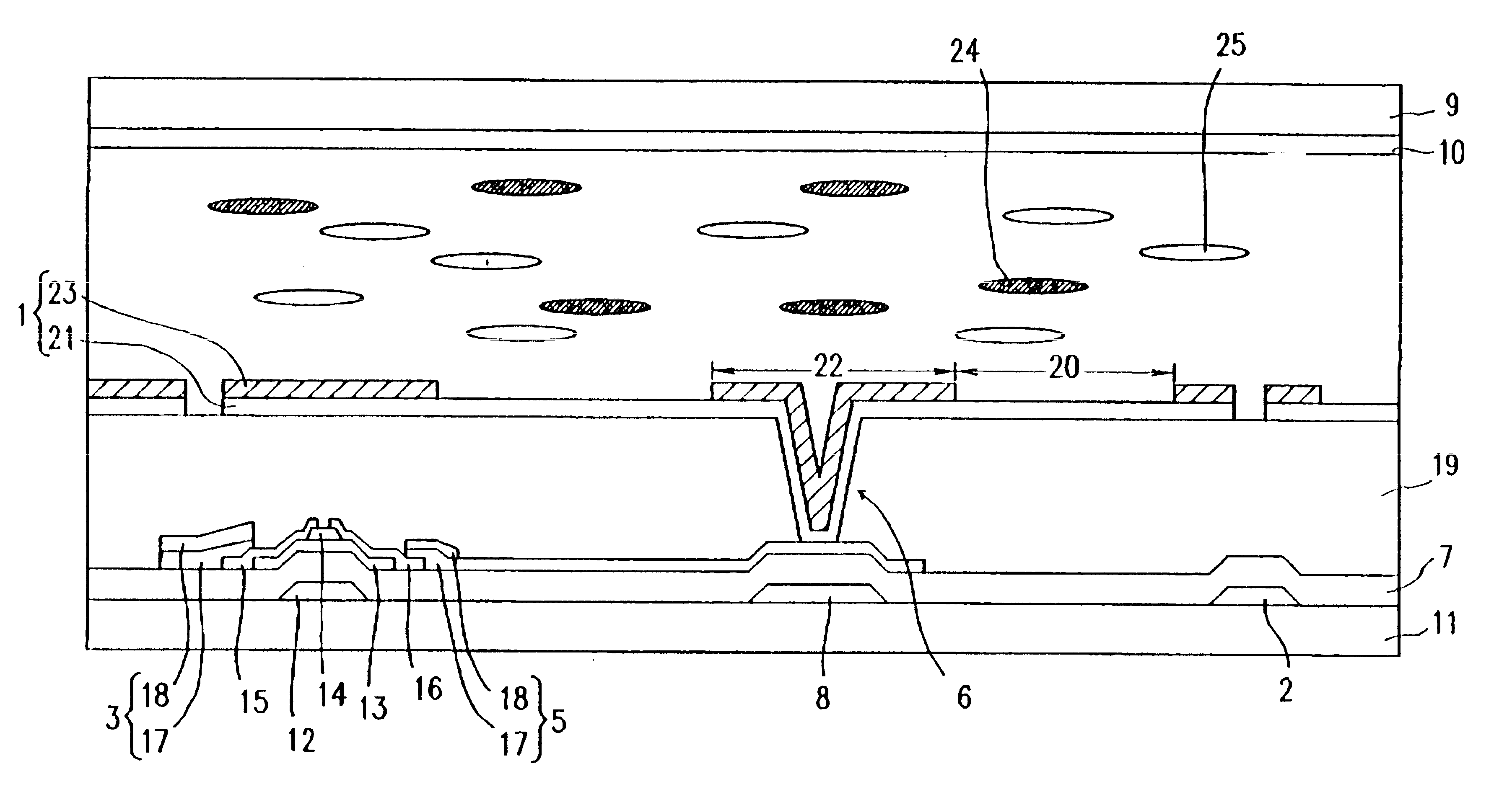
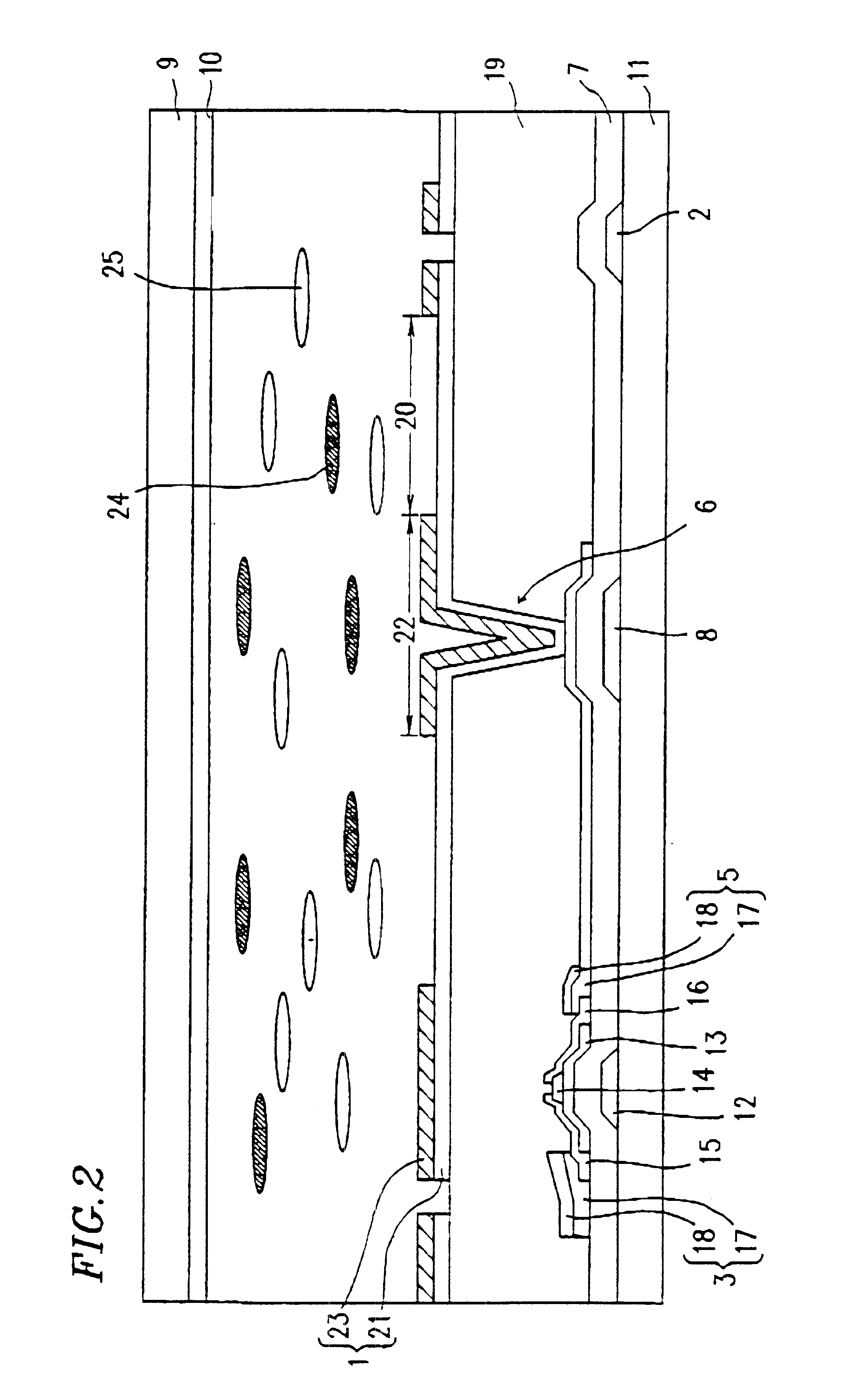
FIG. 7 is a sectional view of a liquid crystal display device of this example according to the present invention. The same components as those of Example 1 are denoted by the same reference numerals as those in FIG. 2.

When the guest-host display method is employed using a mixture of a guest-host liquid crystal material, ZLI 2327 (manufactured by Merck & Co., Inc.) containing black pigments therein and 0.5% of an optically active substance, S-811 (manufactured by Merck & Co., Inc.), the following problem arises. That is, if the optical path length dt of transmitted light from the blacklight in the transmission region using the backlight is significantly different from the optical path length 2dr of reflected light from ambient light in the reflection region, the brightness and the contrast of the resultant display are significantly different between the case where light from the ...

example 4

FIG. 8A is a plan view of one pixel portion of an active matrix substrate of a liquid crystal display device of Example 4 according to the present invention. FIG. 8B is a sectional view taken along line A--A of FIG. 8A.

The active matrix substrate of this example includes gate lines 41, data lines 42, driving elements 43, drain electrodes 44, storage capacitor electrodes 45, a gate insulating film 46, an insulating substrate 47, contact holes 48, an interlayer insulating film 49, reflection pixel electrodes 50, and transmission pixel electrodes 51.

Each of the storage capacitor electrodes 45 is electrically connected to the corresponding drain electrode 44 and overlaps the corresponding gate line 41 via the gate insulating film 46. The contact holes 48 are formed through the interlayer insulating film 49 to connect the transmission pixel electrodes 51 and the storage capacitor electrodes 45.

Each pixel of the active matrix substrate with the above construction includes a reflection pix...


PUM

PropertyMeasurementUnit
thicknessaaaaaaaaaa
transmittanceaaaaaaaaaa

Abstract

A liquid crystal display device according to the present invention includes a first substrate, a second substrate, and a liquid crystal layer interposed between the first substrate and the second substrate. The first substrate includes: a plurality of gate lines; a plurality of source lines arranged to cross with the plurality of gate lines; a plurality of switching elements disposed in the vicinity of crossings of the plurality of gate lines and the plurality of source lines; and a plurality of pixel electrodes connected to the plurality of switching elements. The second substrate includes a counter electrode. A plurality of pixel regions are defined by the plurality of pixel electrodes, the counter electrode, and the liquid crystal layer interposed between the plurality of pixel electrodes and the counter electrode, and each of the plurality of pixel regions includes a reflection region and a transmission region.

Description

The present invention relates to a liquid crystal display device and a method for fabricating the liquid crystal display device. More particularly, the present invention relates to a liquid crystal display device having a transmission display region and a reflection display region in each pixel, and a method for fabricating such a liquid crystal display device.DESCRIPTION OF THE RELATED ARTDue to the features of being thin and consuming low power, liquid crystal display devices have been used in a broad range of fields including office automation (OA) apparatuses such as wordprocessors and personal computers, portable information apparatuses such as portable electronic schedulers, and a camera-incorporated VCR provided with a liquid crystal monitor.Such liquid crystal display devices include a liquid crystal display panel which does not emit light itself, unlike a CRT display and an electroluminescence (EL) display. Therefore, a so-called transmission type is often used as the liqui...

Claims


Application Information

Patent Timeline
Patent Type & Authority Patents(United States)
IPC IPC(8): G02F1/13G02F1/1335G02F1/1343G02F1/137G02F1/139G02F1/1362G02F1/133G02F1/13363
CPCG02F1/133555G02F1/13439G02F1/133526G02F1/136209G02F1/136227G02F1/13725G02F2001/133638G02F2001/13712G02F1/133638G02F1/13712
Inventor KUBO, MASUMINARUTAKI, YOZOBAN, ATSUSHISHIMADA, TAKAYUKIYOSHIMURA, YOJIKATAYAMA, MIKIOISHII, YUTAKANISHIKI, HIROHIKO
Owner SHARP KK
Why Eureka
Try Eureka