
Open drain driver having enhanced immunity to I/O ground noise

a technology of open drain and driver, applied in the field of bus drivers, can solve the problems of core and input noise margin, rapid current change of power and ground bus, and undershoot noise on the vss_ext lin

Inactive Publication Date: 2002-10-29
SONY CORP +1
View PDF4 Cites 9 Cited by
  • Summary
  • Abstract
  • Description
  • Claims
  • Application Information

AI Technical Summary

Problems solved by technology

When the external reference voltage VSS_EXT is connected to simultaneously switching outputs (SSO) circuitry, undershoot noise can occur on the VSS_EXT line.
SSO is a well-known potential source of system noise, and SSO noise is often the largest component in the noise budget.
Specifically, SSO causes rapid current changes in the power and ground buses.
Because of supply pin inductance, this current change causes bus voltage fluctuation, and thus reduces core and input noise margins.
This noise can cause the driver circuit to generate false logic states, which is highly undesirable.
In general, these modifications are undesirable due to constraints they can place on circuit density, layout and cost of implementation.

Method used


Image

  • Open drain driver having enhanced immunity to I/O ground noise
  • Open drain driver having enhanced immunity to I/O ground noise
  • Open drain driver having enhanced immunity to I/O ground noise

Examples


Embodiment Construction

The following description is not to be taken in a limiting sense, but is made for the purpose of describing the general principles of the invention. The scope of the invention should be determined with reference to the claims.

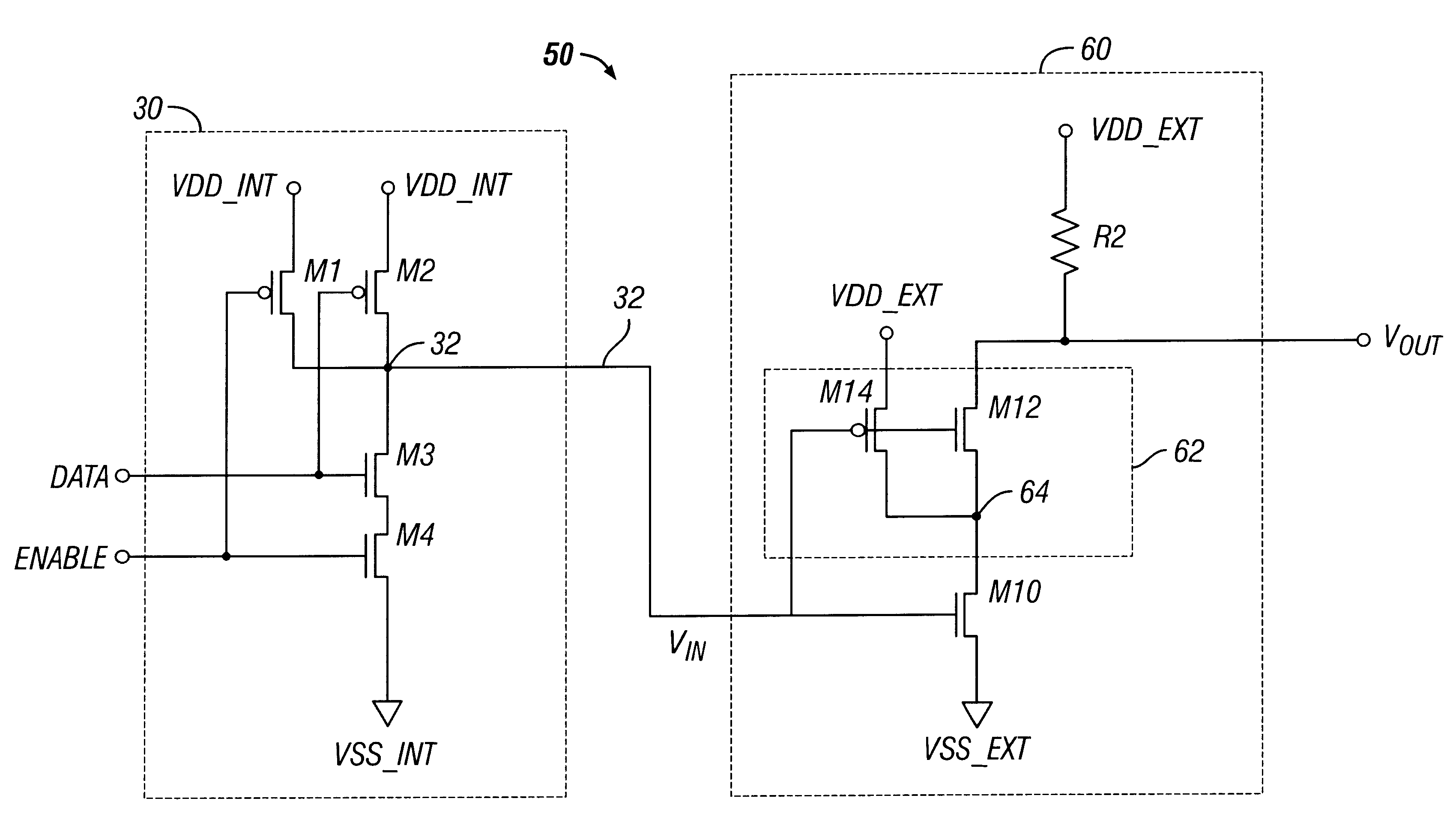
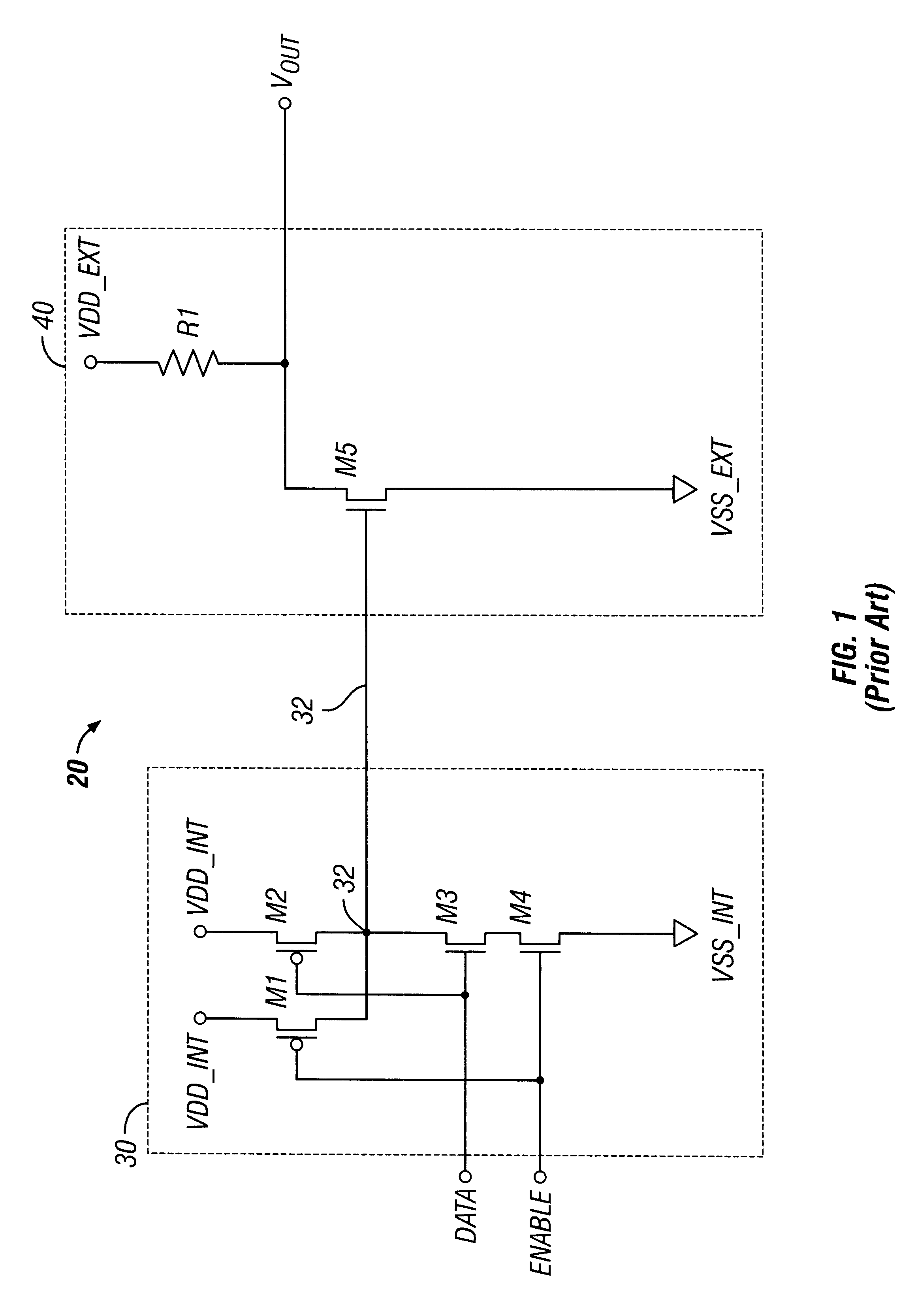
This description begins with a detailed discussion of the operation of the bus driver 20 shown in FIG. 1. The bus driver 20 includes a CMOS NAND gate 30 followed by an open drain I / O driver 40. The inputs of the NAND gate 30 are labeled DATA and ENABLE. The output of the NAND gate 30 is generated at node 32, which also serves as the input of the open drain I / O driver 40. The output of the open drain I / O driver 40 is labeled V.sub.OUT.

When DATA and ENABLE are both high, transistors M1 and M2 are both turned off, while transistors M3 and M4 are both turned on. These input conditions result in the output node 32 being pulled down to VSS_INT. When DATA and ENABLE are both low, transistors M3 and M4 are both turned off, while transistors M1 and M2 are both turned on...


PUM


Abstract

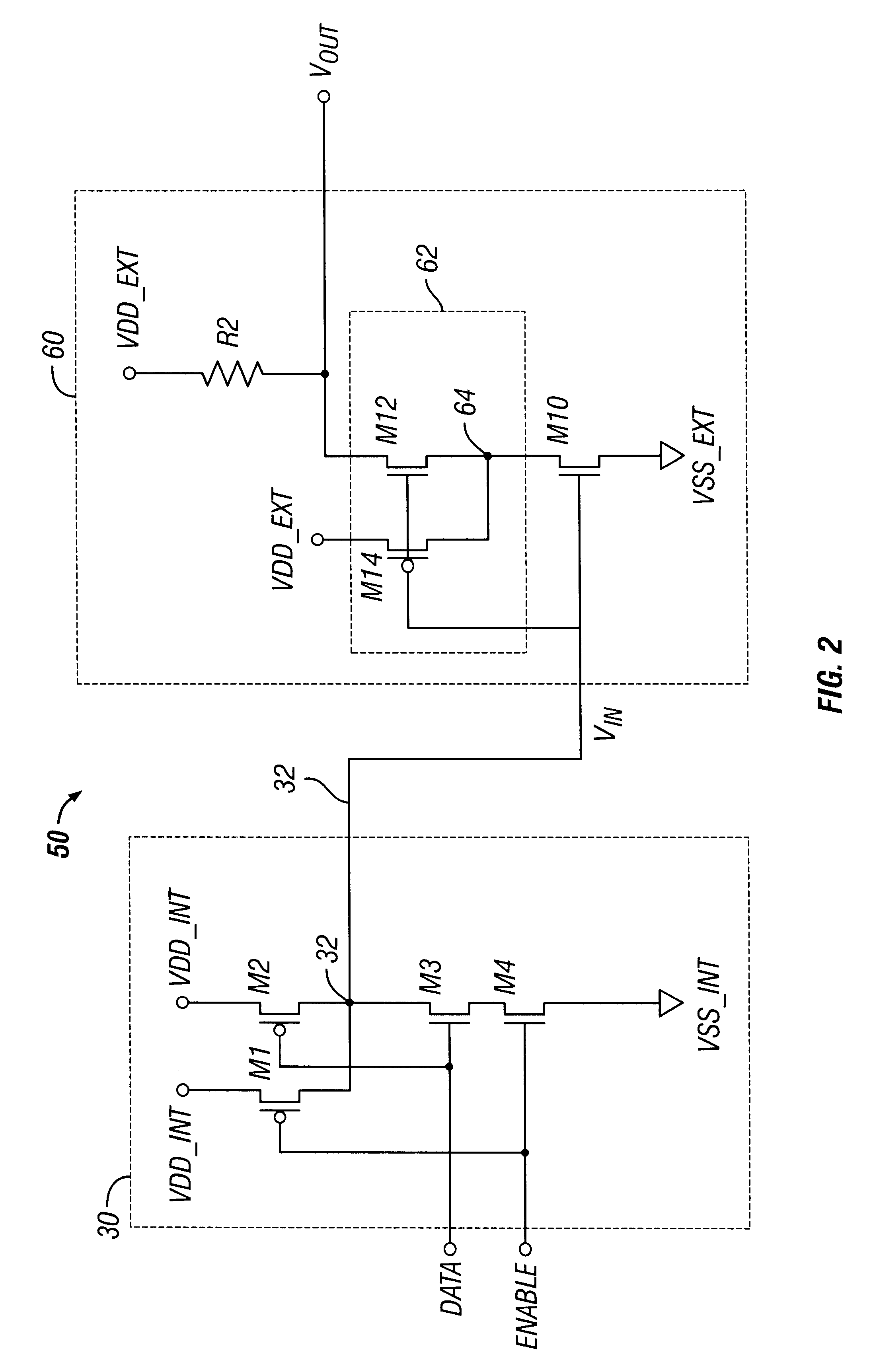
An open drain I / O driver includes an input node, an output node, a first reference node, a first transistor, and noise immunity circuitry. The first transistor has its gate coupled to the input node and its conducting path coupled in series with the output node and the first reference node. The first transistor operates to uncouple the output node from the first reference node in response to an input voltage applied to the input node. The noise immunity circuitry keeps the output node uncoupled from the first reference node during undershoot noise in a first reference voltage that causes the first transistor to change from an off state to an on state. The noise immunity circuitry includes second and third transistors. The second transistor has its gate coupled to the input node and its conducting path coupled in series with the conducting path of the first transistor. The third transistor is configured to keep the second transistor in an off state during the undershoot noise.

Description

1. Field of the InventionThe present invention relates generally to bus drivers used in digital electronics, and more specifically to CMOS open drain bus drivers.2. Discussion of the Related ArtA bus driver is a circuit that amplifies a bus data or control signal sufficiently to ensure valid reception of that signal at the destination. Bus drivers, which are typically controlled with normal logic levels, increase the driving capability of other devices, such as microprocessors, which themselves may be capable of driving no more than a single load.FIG. 1 illustrates a conventional complementary metal-oxide semiconductor (CMOS) bus driver 20. The driver 20 includes a NAND gate 30 and an open drain I / O driver 40. The NAND gate 30 includes p-channel transistors M1, M2, and n-channel transistors M3, M4, all connected substantially as shown. The DATA input is coupled to the gates of transistors M2, M3, and the ENABLE input is coupled to the gates of transistors M1, M4. The drains of trans...

Claims


Application Information

Patent Timeline
Patent Type & Authority Patents(United States)
IPC IPC(8): H03K17/16H03K19/003
CPCH03K17/162H03K19/00361
Inventor SANWO, IKUO JIMMYNEJAT, MAHYARCLERGE, JEAN-ROBERT
Owner SONY CORP
Learn More