Timing analysis apparatus and method for semiconductor integrated circuit in consideration of power supply and ground noises

a timing analysis and integrated circuit technology, applied in the field of timing analysis apparatus and method for use in semiconductor integrated circuits, can solve the problems of insufficient analysis accuracy and delay time, and achieve the effects of high accuracy timing design, simplified calculation step of delay time, and increased accuracy

Inactive Publication Date: 2011-09-13
SEMICON TECH ACADEMIC RES CENT
View PDF7 Cites 8 Cited by
  • Summary
  • Abstract
  • Description
  • Claims
  • Application Information

AI Technical Summary

Benefits of technology

[0033]Therefore, according to the timing analysis apparatus for use in semiconductor integrated circuit and method of the present invention, the delay value of the logic gates, that constitutes the semiconductor integrated circuit such as a digital LSI can be calculated in consideration of the static and dynamic power supply noises. In addition, by handling the action of the relative relation between the noise waveform and the logic gate operation on the time base or the temporal axis as the fluctuation width of the delay time, and performing calculation of the delay time in the semiconductor integrated circuit dividedly at each frequency, the accuracy is increased. Further, the calculation step of the delay time is largely simplified to execute these steps by the ability of the existent computer, and therefore, highly accurate timing design can be achieved in a short time.

Problems solved by technology

Fluctuations in the voltage of the power wiring and ground wiring generated in the operation of such a digital LSI, i.e., the power supply noises are actualized by a reduction in the power supply voltage caused by the scale shrinkage and becomes unignorable.
However, the fluctuation components in a cycle equivalent to or shorter than the switching operation time (i.e., high frequency) are operative as dynamic changes in the effective power supply and ground voltages in the process of the switching operation of the logic gate, and a current change due to this fluctuates the delay time.
As described above, the conventional timing analysis method, which does not include the calculation of the delay time in consideration of the temporal fluctuations of the power supply noise and the ground noise, has therefore been unable to obtain sufficient analysis accuracy.

Method used


Image

  • Timing analysis apparatus and method for semiconductor integrated circuit in consideration of power supply and ground noises
  • Timing analysis apparatus and method for semiconductor integrated circuit in consideration of power supply and ground noises
  • Timing analysis apparatus and method for semiconductor integrated circuit in consideration of power supply and ground noises

Examples


Embodiment Construction

[0061]Preferred embodiments of the present invention will be described below with reference to the drawings. In each of the following preferred embodiments, like components are denoted by like reference numerals.

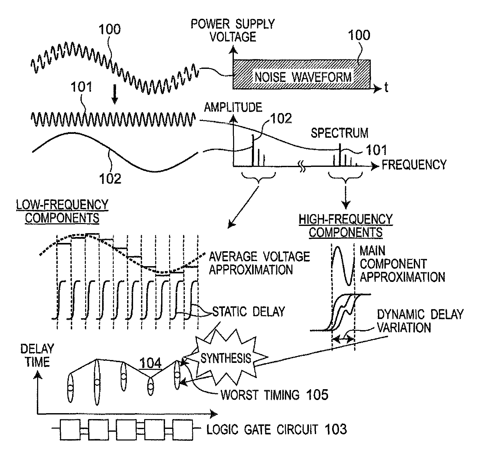
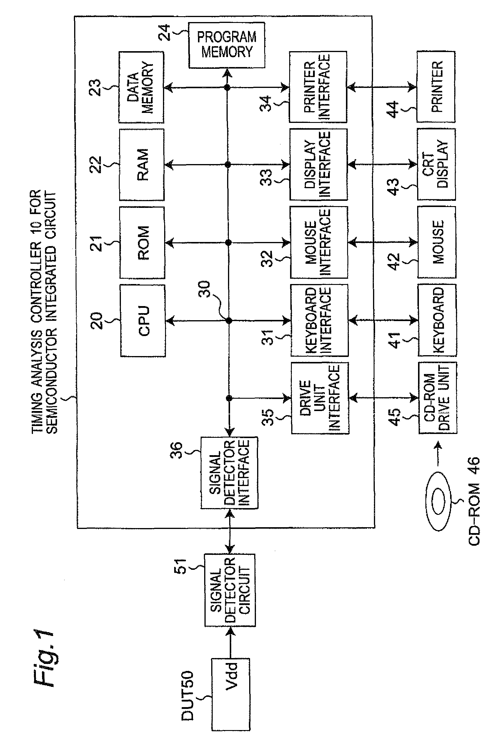
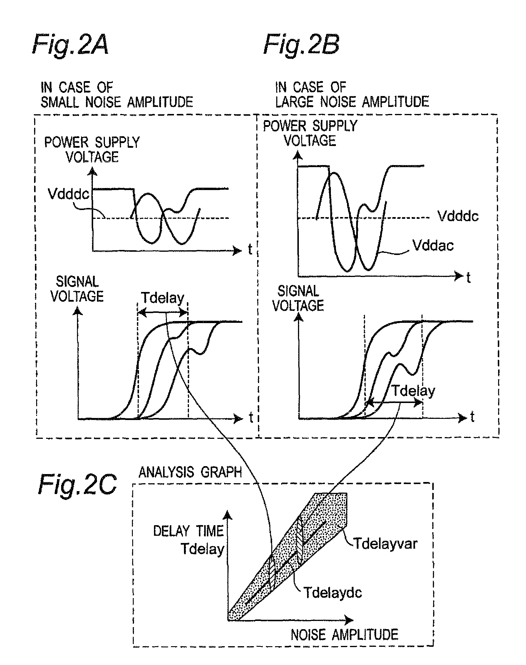
[0062]FIG. 1 is a block diagram showing a configuration of a timing analysis apparatus for use in semiconductor integrated circuit according to one preferred embodiment of the present invention. As shown in FIG. 1, the timing analysis apparatus for use in semiconductor integrated circuit according to the present preferred embodiment is configured so as to include a timing analysis controller 10 of the semiconductor integrated circuit of a digital computer. By executing calculation and processing of the delay time of the logic gates in the timing analysis in consideration of the dynamic power supply noise of FIG. 6, calculation and processing of the delay time of the logic gates in a digital circuit design in consideration of the dynamic power supply noise of FIG. 7 or the di...


PUM


Abstract

In a timing analysis apparatus for use in a semiconductor integrated circuit, which analyzes operation timing of a semiconductor integrated circuit having a logic gate circuit including a plurality of logic gates, a controller detects at least one of a power supply voltage and a ground voltage of a power supply, decomposes the noise waveform into frequency components, classifies the frequency components into low-frequency components lower than a predetermined threshold frequency and high-frequency components higher than the threshold frequency, calculates a static delay time of each of the logic gates due to the low-frequency components, calculates a dynamic delay time of each of the logic gates due to the high-frequency components, and determines a delay time of each of the logic gates by synthesizing the calculated respective delay times.

Description

BACKGROUND OF THE INVENTION[0001]1. Field of the Invention[0002]The present invention relates to a timing analysis apparatus and method for use in semiconductor integrated circuits and, in particular, to a timing analysis apparatus and method for calculating the delay time of logic gates in a semiconductor large-scale digital integrated circuit (LSI) in consideration of fluctuations in power supply and ground voltages of LSI, i.e., influences of power supply and ground noises.[0003]2. Description of the Related Art[0004]In accordance with developments in the semiconductor manufacturing process, a large amount of logic gate circuit employing submicron transistors are integrated at high density in a digital LSI. Fluctuations in the voltage of the power wiring and ground wiring generated in the operation of such a digital LSI, i.e., the power supply noises are actualized by a reduction in the power supply voltage caused by the scale shrinkage and becomes unignorable. The effective powe...

Claims


Application Information

Patent Timeline
Patent Type & Authority Patents(United States)
IPC IPC(8): G06F17/50
CPCG06F17/5031G06F30/3312
Inventor NAGATA, MAKOTO
Owner SEMICON TECH ACADEMIC RES CENT
Why Eureka
Try Eureka