Semiconductor integrated circuit device

a technology of integrated circuits and semiconductors, applied in logic circuit coupling/interface arrangements, pulse techniques, instruments, etc., can solve the problems of low processing speed of circuits, low detection accuracy, and low speed of high-speed operation, and achieve accurate detection

Inactive Publication Date: 2002-12-03
RENESAS ELECTRONICS CORP
View PDF9 Cites 28 Cited by
  • Summary
  • Abstract
  • Description
  • Claims
  • Application Information

AI Technical Summary

Benefits of technology

As a layout of the circuit, the speed controller is comprised of the delay detector and the controller. When the delay detector is disposed in the block to be controlled, particularly, in the center of the block, the operating speed can be accurately detected.
As another mode of the invention, there is provided a semiconductor integrated circuit device comprising a logic circuit for performing a predetermined process, an input / output circuit for transmitting a signal to the logic circuit, and a speed controller for controlling the operating speed of the circuit, characterized in that the signal transmitting speed of the input / output circuit is controlled by the speed controller. Specifically, the speed controller controls the substrate bias of the transistor constructing the input / output circuit to change the threshold, thereby controlling the operating speed.

Problems solved by technology

By an increase in the range of variation, even if the device becomes finer, high-speed operation is limited by the worst delay.
In this case, there is a drawback such that the ON current of the MOS transistor conspicuously decreases by deterioration in mobility and increase in the threshold due to the temperature rise, and as a result, the processing speed of the circuit decreases.
Since it takes a few .mu. seconds until an output voltage of the filter is stabilized, stabilization time of a control signal is long, and the signal tends to be unstable.
Consequently, control accuracy cannot be raised.
When the capacitance and the inductance used for the filter are formed on the same chip on which a circuit to be controlled is also mounted, the fact that they occupy a large area becomes a problem.

Method used


Image

  • Semiconductor integrated circuit device
  • Semiconductor integrated circuit device
  • Semiconductor integrated circuit device

Examples


Embodiment Construction

Embodiments of the invention will be described hereinbelow with reference to the drawings.

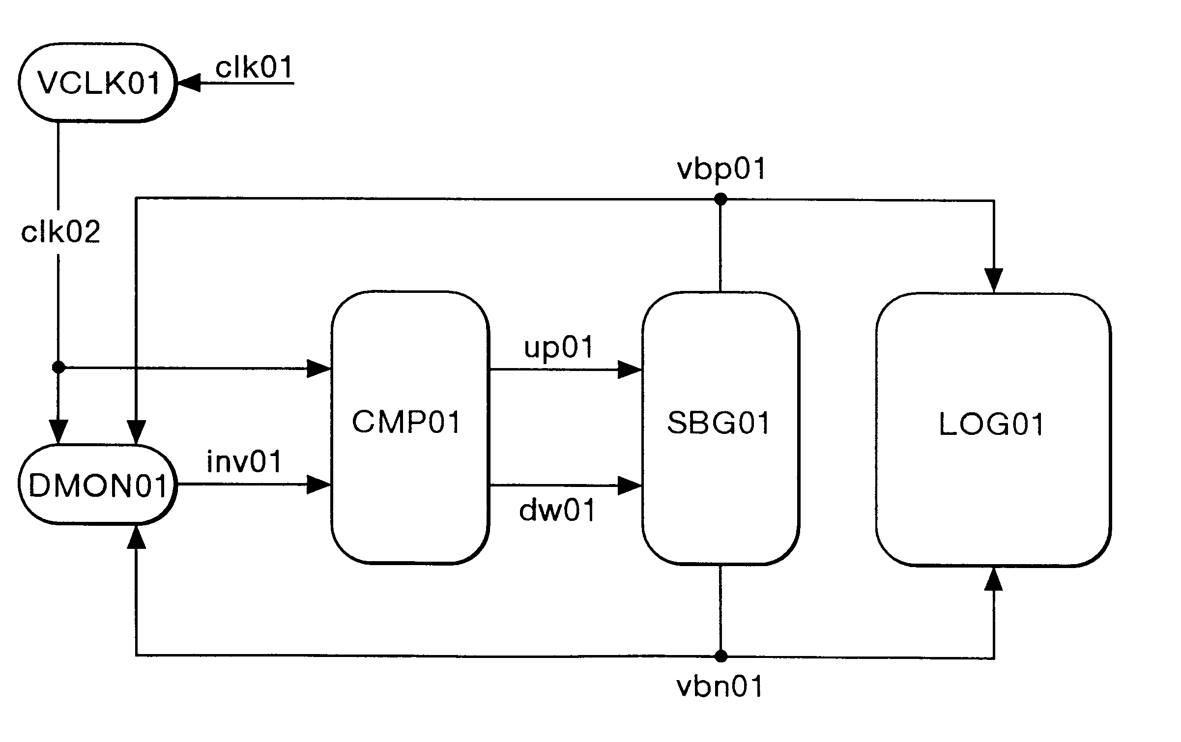
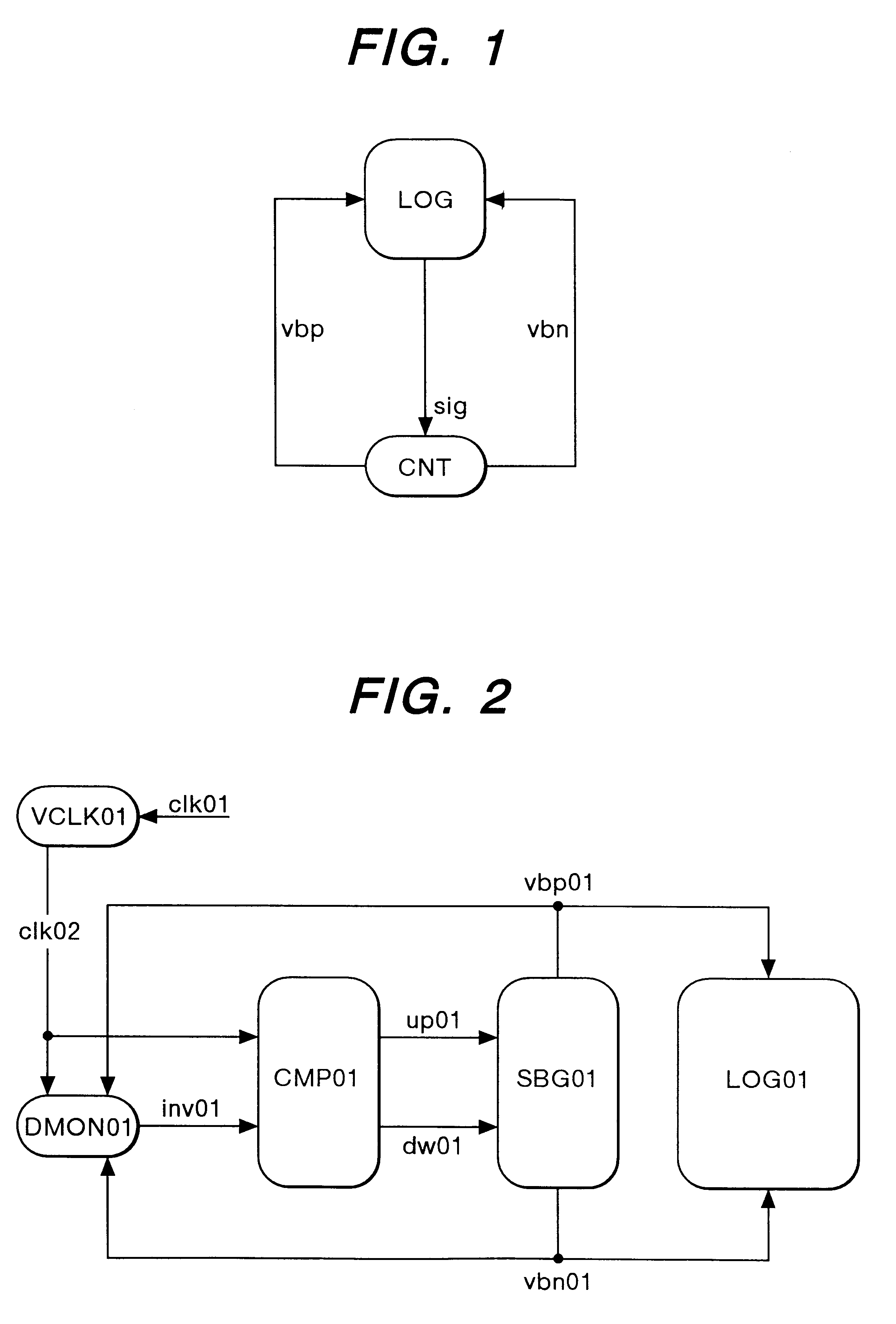
FIG. 1 is a diagram showing the fundamental concept of the invention. A main circuit LOG transmits a detected signal sig according to the operating speed of the circuit to a substrate-bias controller CNT. The substrate-bias controller CNT supplies both a substrate vias vbp for a p-channel type MOSFET and a substrate vias vbn for an n-channel type MOSFET to the main circuit LOG. The main circuit LOG is constructed by an MOS transistor. By controlling the substrate bias of the MOS transistor, a threshold voltage is controlled.

With such a construction, even when the characteristics of the MOS transistor fluctuate, due to variations in temperature and supply voltage or variations in the fabrication process of the MOS transistor, by controlling the substrate bias to control the threshold voltage of the MOS transistor, the operating speed can be made always constant. Further, the MOS transistor is fa...


PUM


Abstract

A semiconductor integrated circuit device includes a logic circuit, a digital-to-analog converter generating a substrate bias for controlling a threshold voltage of an MIS transistor of the logic circuit, a voltage control circuit outputting a control signal in accordance with a delay signal, and a delay detector, including a circuit which monitors variations in operating speed of the delay detector. The delay detector receives the clock signal and outputs the delay signal. The voltage control circuit receives the delay signal and outputs the control signal according to a delay indicated by the delay signal. The digital-to-analog converter receives the control signal from the voltage control circuit and generates a voltage according to the control signal. The operating speed of each of the logic circuits and the delay detector is controlled by a voltage supplied from the digital-to-analog converter.

Description

The present invention relates to a semiconductor integrated circuit, and, more particularly, a semiconductor integrated circuit device suitable for high-speed operation.In an integrated circuit using CMOS transistors, characteristics fluctuation exists due to variations in transistor dimension caused by a fabrication process and a change in the environment, such as temperature or supply voltage, during operation.As described in "1994 symposium on VLSI technology digest of technical papers" (June, 1994), pp. 13 to 14, as an MOS transistor becomes finer, fluctuation in basic parameters, such as a threshold value due to the characteristics fluctuation caused by a fabrication process, becomes larger.FIG. 12 schematically shows delay of a CMOS circuit with respect to the device feature size of a MOS transistor and the range of variation. In designing a CMOS integrated circuit, the worst delay in FIG. 12 has to be considered. By an increase in the range of variation, even if the device be...

Claims


Application Information

Patent Timeline
Patent Type & Authority Patents(United States)
IPC IPC(8): H03K19/003H03K3/01H03K19/0185
CPCH03K19/00323H03K19/00384H03K19/018585
Inventor MIYAZAKI, MASAYUKIISHIBASHI, KOICHIROMIZUNO, HIROYUKI
Owner RENESAS ELECTRONICS CORP
Why Eureka
Try Eureka