Method and apparatus for fixed abrasive substrate preparation and use in a cluster CMP tool

a technology of fixed abrasives and tools, which is applied in the field of method and apparatus for fixing abrasive substrate preparation and use in cluster cmp tools, can solve the problems of high system ownership cost for users, inconsistent results of fixed abrasives, and too abrasive rough polishing to afford the necessary planarization control, so as to improve reliability, reduce the cost of a cmp system, and improve the effect of abrasive material control

Inactive Publication Date: 2002-12-17
APPLIED MATERIALS INC
View PDF66 Cites 14 Cited by
  • Summary
  • Abstract
  • Description
  • Claims
  • Application Information

AI Technical Summary

Benefits of technology

It is therefore an advantage of the present invention to increase the reliability and decrease the cost of a CMP system by providing an arrangement and method to better control the amount of abrasive material used during planarization of a semiconductor wafer. An additional advantage of the present invention is the improvement in process control of the planarization of the semiconductor wafer.

Problems solved by technology

During device fabrication, only CMP is used as rough polishing is too abrasive to afford the necessary planarization control.
At least one of the problems with these current fixed-abrasive CMP systems is similar to that of more-conventional slurry-type systems; a high cost of ownership of the system for the user.
Additional problems include both inconsistent results of the fixed abrasive as the abrasive wears away due to usage and reliance on third-party produced consumable abrasive or slurry material.

Method used


Image

  • Method and apparatus for fixed abrasive substrate preparation and use in a cluster CMP tool
  • Method and apparatus for fixed abrasive substrate preparation and use in a cluster CMP tool
  • Method and apparatus for fixed abrasive substrate preparation and use in a cluster CMP tool

Examples


Embodiment Construction

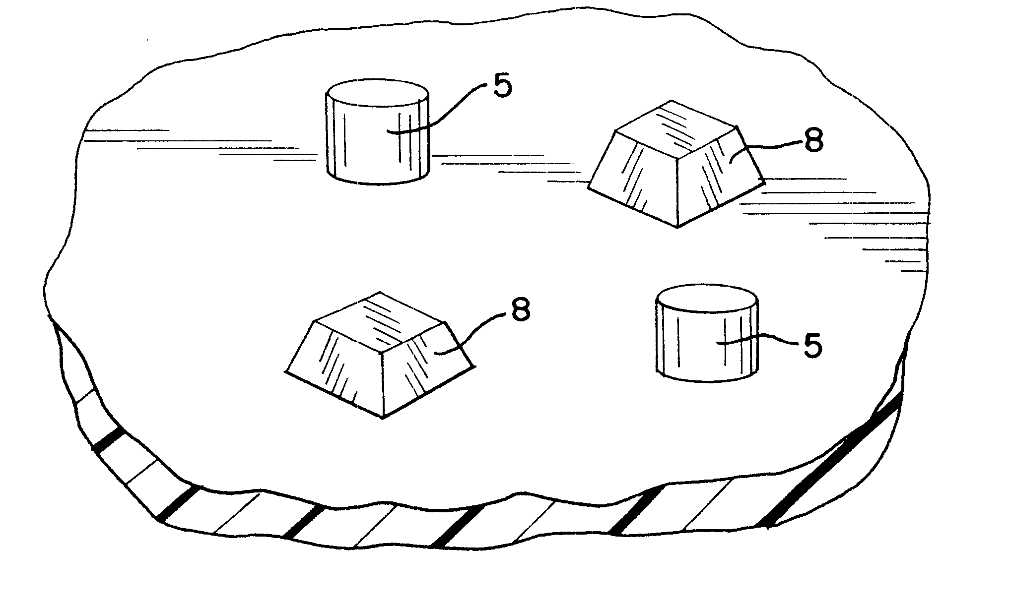
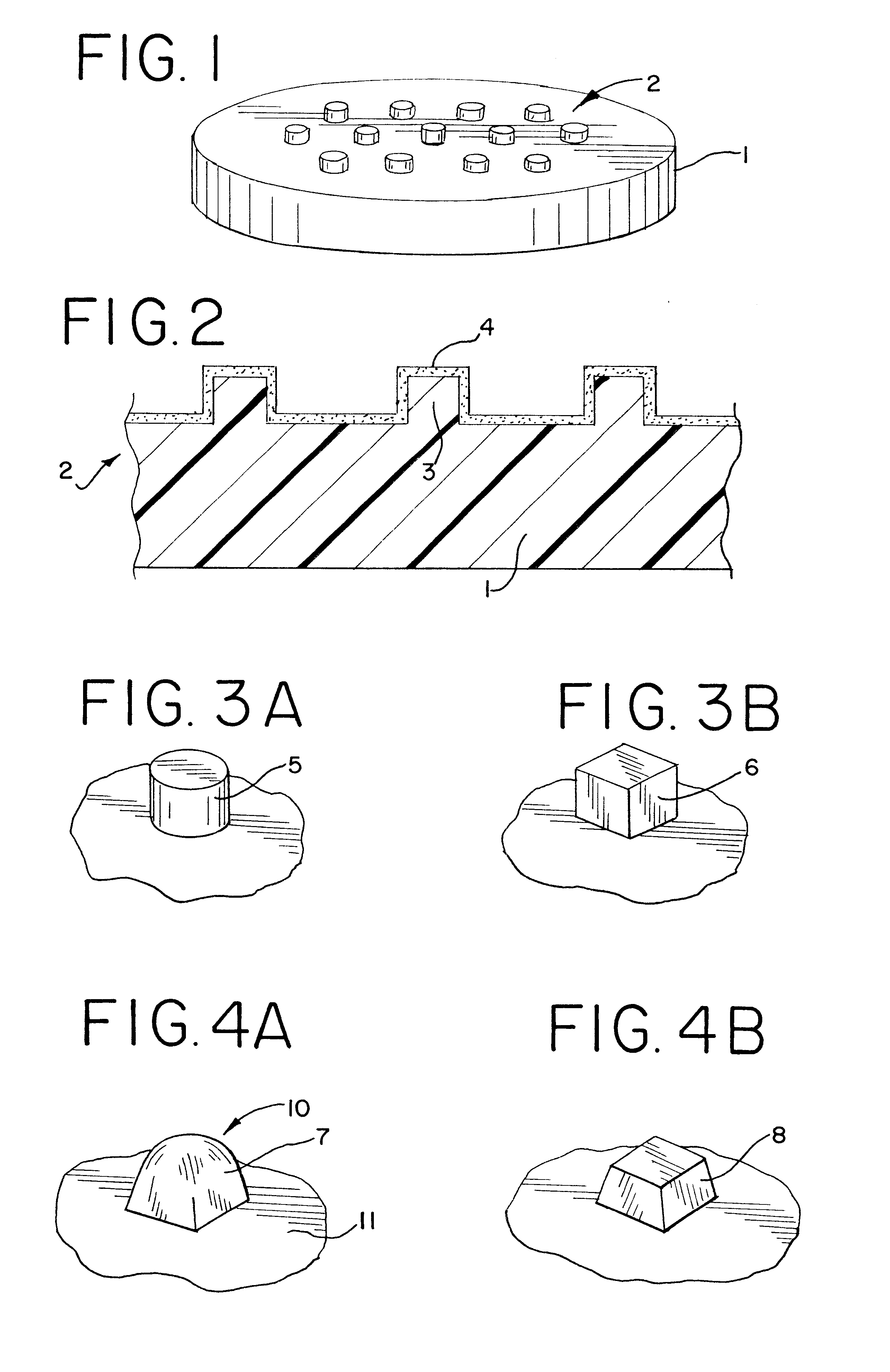
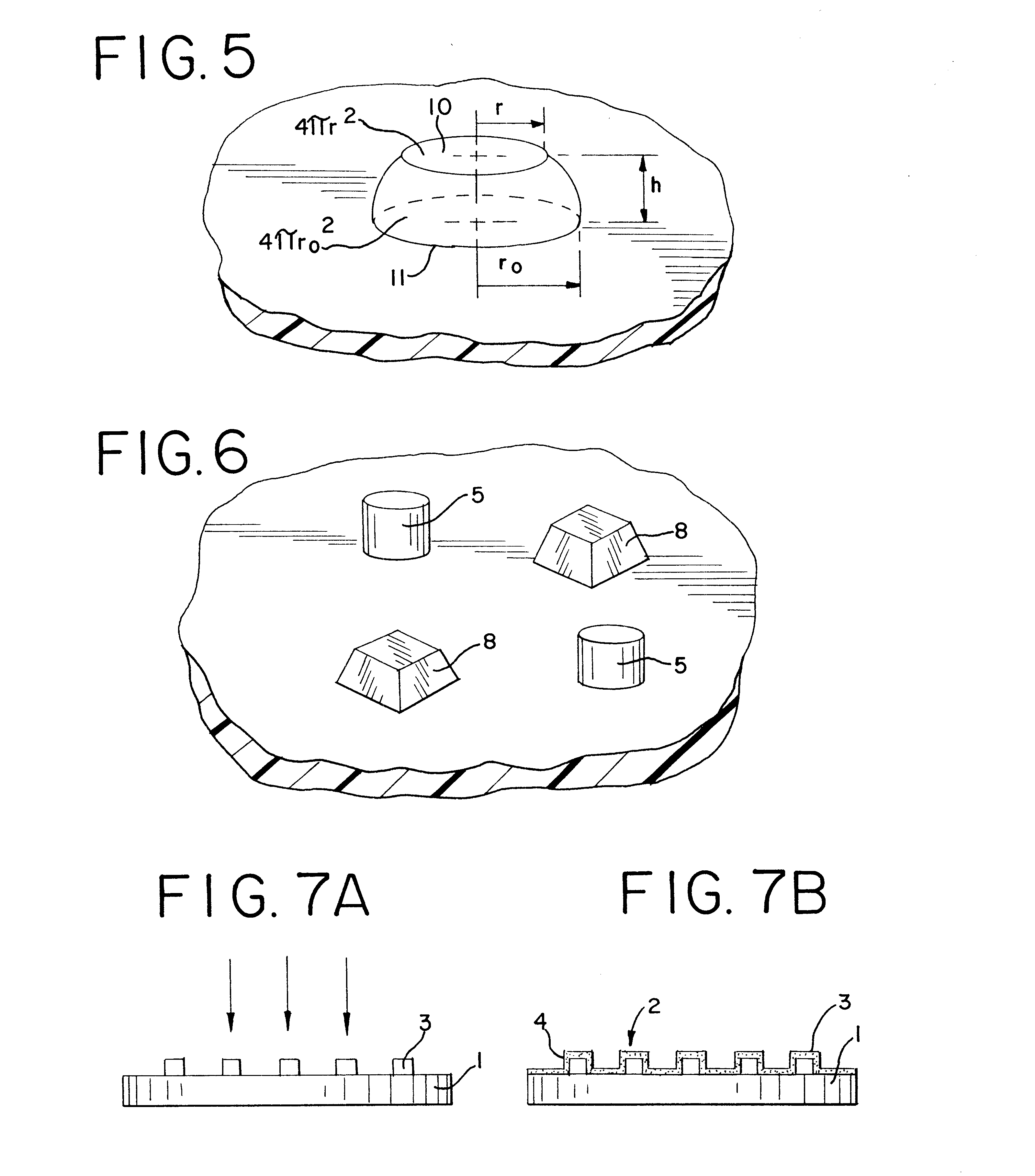
FIGS. 1 and 2 depict top and side views of a preferred embodiment of a fixed abrasive substrate according to the present invention. In FIG. 1, a substrate 1 is provided with an abrasive-coated predetermined pattern 2. FIG. 2 depicts a side view of the coated substrate 1 better showing the abrasive-coated predetermined pattern 2, which consists of a predetermined pattern 3 and a fixed abrasive 4 coating the pattern 3.

The substrate 1 is made of a durable material that is suitable for use in a standard vacuum deposition process. Examples of typical materials include, but are not limited to, ceramic, rigid plastic or other rigid material such as polyethylene terephthalate (PET). The substrate is generally purchased from a vendor of the particular material that comprises the substrate.

The substrate pattern is a three-dimensional topographical pattern that may be prepared by a number of different methods, including physically or chemically etching the substrate to form the pattern or depo...


PUM

PropertyMeasurementUnit
widthaaaaaaaaaa
heightaaaaaaaaaa
widthaaaaaaaaaa

Abstract

A method of creating and using a polishing substrate having a coating layer that includes providing a substrate having a predetermined pattern disposed on a surface of the substrate and coating the surface of the substrate with an abrasive to form a coated substrate conforming to the predetermined pattern is described. In addition, an apparatus enabling preparation and use of a fixed abrasive polishing member is described that includes a patterned substrate, an abrasive coating a surface of the patterned substrate and a vacuum deposition chamber in which the abrasive is applied to the surface of the substrate. In addition, rather than a fixed abrasive, non-abrasive material may be applied to the surface of the patterned substrate, in which case, a conventional slurry may be used in planarization of an applied semiconductor wafer.

Description

The present invention relates to the field of fixed abrasive substrates. More particularly, the invention relates to a method and apparatus for fixed abrasive preparation and use in a cluster chemical-mechanical polishing (CMP) tool.One of the last stages before fabrication of semiconductor devices on a semiconductor substrate, such as Si or III-V related compounds (e.g. GaAs, InP), involves the polishing of the semiconductor wafer. One reason wafer polishing is performed is to remove any irregularities present on the surface so that the wafer is smooth and flat prior to performing any initial fabrication steps (such as etch, metalization or photolithography). In addition, CMP is also used to planarize the semiconductor wafer subsequent to initiation of device fabrication, for example after deposition of polyamide or other insulating material on the wafer.In general, prior to device fabrication, there are two types of polishing: rough polishing and chemical-mechanical polishing (CMP...

Claims


Application Information

Patent Timeline
Patent Type & Authority Patents(United States)
IPC IPC(8): C23F1/00H01L21/306H01L21/302H01L21/02H01L21/461B24B7/22B24D11/00
CPCB24B7/228B24D11/001
Inventor BOYD, JOHN M.LACY, MICHAEL S.
Owner APPLIED MATERIALS INC
Why Eureka
Try Eureka