Ferroelectric memory device having a protective layer
- Summary
- Abstract
- Description
- Claims
- Application Information
AI Technical Summary
Problems solved by technology
Method used
Image

Examples
first embodiment
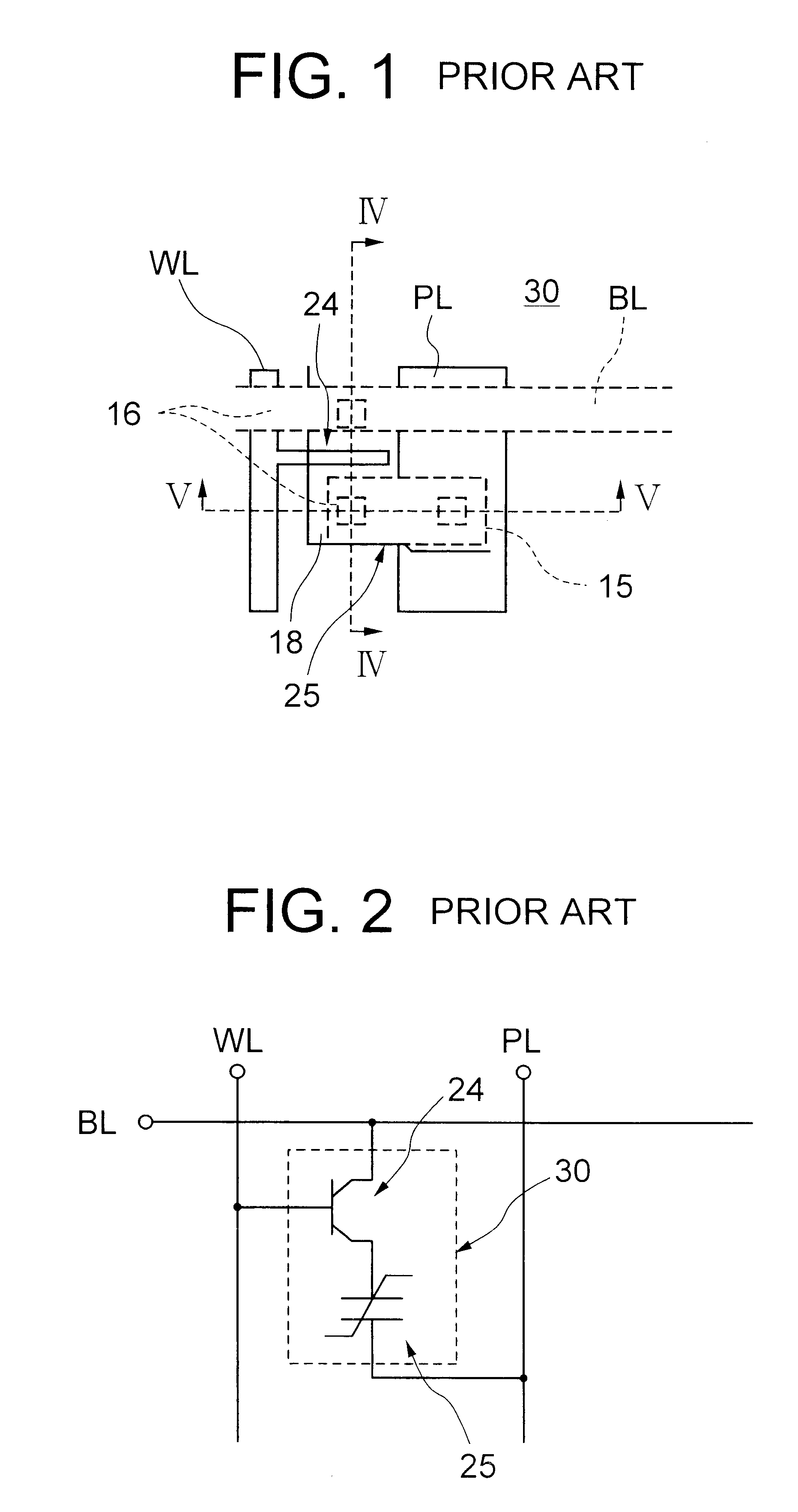
A ferroelectric memory device according to a first embodiment of the present invention includes a memory cell array including a plurality of memory cells arranged in a matrix, a peripheral circuit disposed adjacent to the memory cell array, and an interconnection structure for connecting the memory cells and the peripheral circuit for storing or reading data in / from the memory cells.
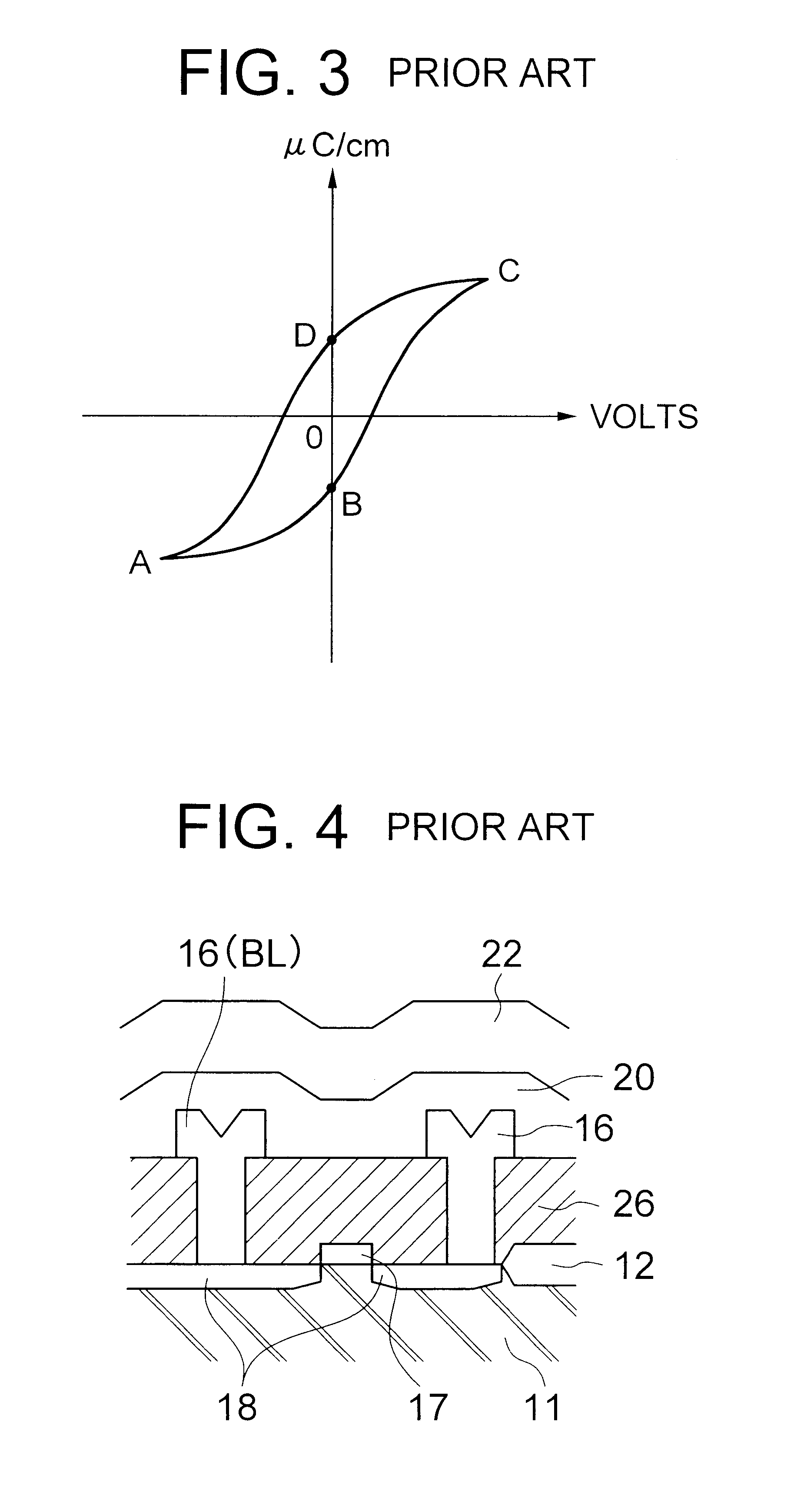
Referring to FIGS. 7, 8 and 9, the memory cell in the ferroelectric memory device according to the present embodiment is similar to the conventional memory cell shown in FIGS. 1, 4 and 5 except for a first protective layer 21 and a second protective layer (insulator layer) 22 consecutively and separately formed on the ferroelectric capacitor.
More specifically, the memory cell includes a cell transistor 24 implemented by a FET, a ferroelectric capacitor 25 disposed above the cell transistor 24 and a cover film 19 covering the ferroelectric capacitor 25. The ferroelectric capacitor 25 includes a bottom ele...
second embodiment
Referring to FIG. 11, a ferroelectric memory device according to a second embodiment of the present invention is similar to the first embodiment except that the bottom electrode 13 is connected to one of the source / drain regions 18 through a silicon via plug 23, and the top electrode 15 is connected to the interconnect layer 16 acting as a plate line. On the interconnect layer 16 is deposited the interlayer dielectric film 20, on which the first protective layer 21 and the second protective layer 22 are consecutively formed.
WSi.sub.x is preferably used for the interconnect layer 16. If Al is to be used, on the other hand, for a lower resistivity of the interconnect layer 16, the interconnect layer preferably includes WSi.sub.x film, TiN film, Al film and TiN film as viewed from the bottom, wherein the TiN film is used for the barrier layer between the Al film and the Si film and the WSi.sub.x film is used for the underlying layer.
The top electrode 15 may be preferably implemented by...
third embodiment
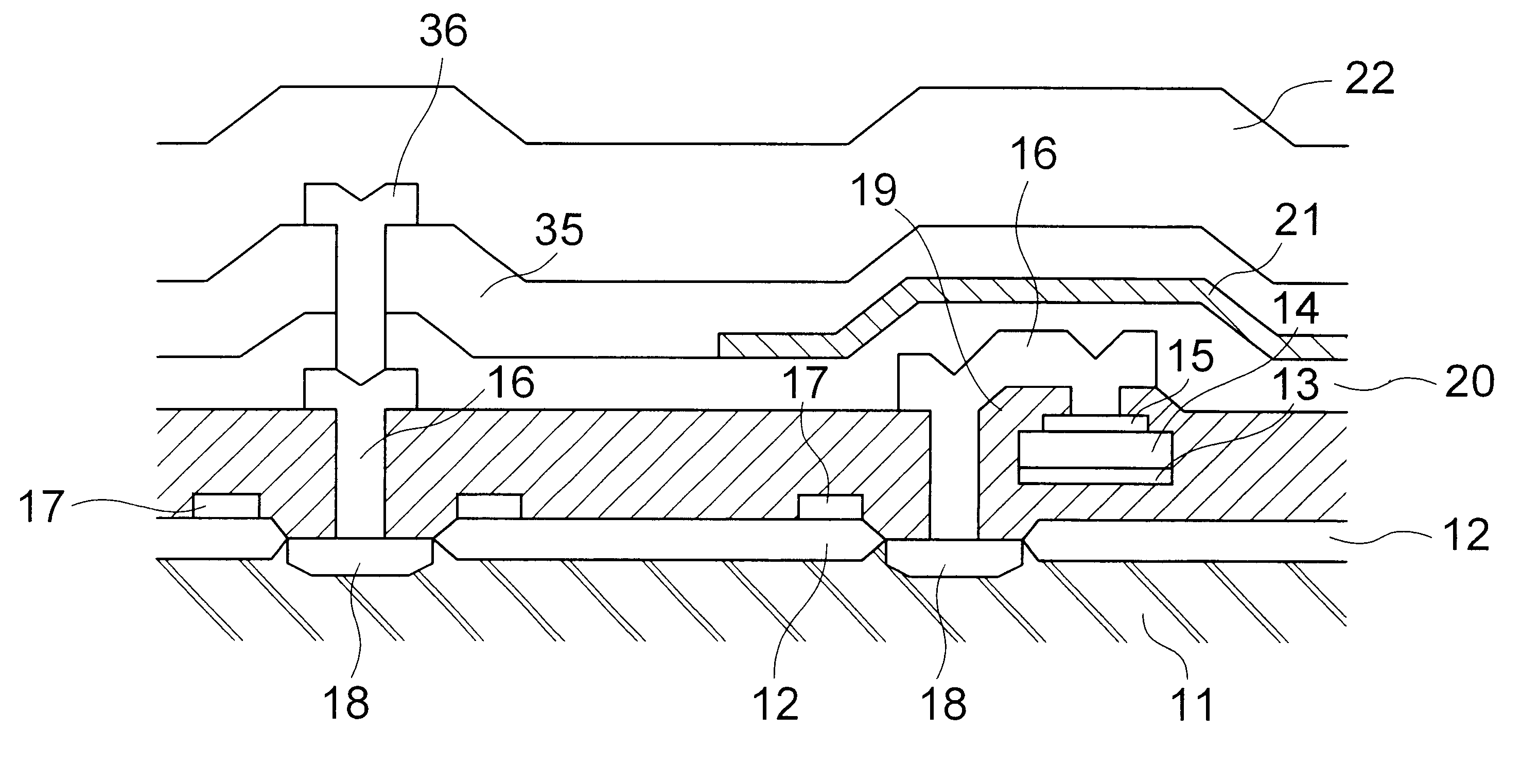
Referring to FIG. 12, a ferroelectric memory device according to a third embodiment of the present invention is similar to the first embodiment except that the first protective layer 21 is formed only in the area for the cell array on another interlayer dielectric film 35, which is formed on the interlayer dielectric film 20 covering the interconnect layer 16. In the present embodiment, a second interconnect layer 36 including Al as a main component thereof is formed on the interlayer dielectric film 20 for implementing the peripheral circuit of the memory device. The first protective layer 21 may be formed at any level so long as the first protective layer 21 is disposed between the interconnect layer 16 overlying the top electrode 15 and the second protective layer 22.
It is sufficient that the first protective layer 21 in the present invention is disposed only just above the memory cell array because the first protective layer 21 is designed only for protection of the ferroelectri...
PUM
 Abstract
Description
Claims
Application Information
 - Generate Ideas
- Intellectual Property
- Life Sciences
- Materials
- Tech Scout
- Unparalleled Data Quality
- Higher Quality Content
- 60% Fewer Hallucinations
Browse by: Latest US Patents, China's latest patents, Technical Efficacy Thesaurus, Application Domain, Technology Topic, Popular Technical Reports.
© 2025 PatSnap. All rights reserved.Legal|Privacy policy|Modern Slavery Act Transparency Statement|Sitemap|About US| Contact US: help@patsnap.com