Semiconductor device and manufacturing method thereof

a technology of semiconductor devices and manufacturing methods, applied in semiconductor devices, capacitors, electrical devices, etc., can solve problems such as difficulty in adjusting etching conditions, and achieve the effect of preventing local damage to ferroelectric films and reducing leakage currents

Inactive Publication Date: 2005-04-28
FUJITSU MICROELECTRONICS LTD
View PDF2 Cites 40 Cited by
  • Summary
  • Abstract
  • Description
  • Claims
  • Application Information

AI Technical Summary

Benefits of technology

[0007] An object of the present invention is to provide a semiconductor device provided with a ferroelectric capacitor of a structure capable of reducing leakage current adequately while preventing local damages to a ferroelectric film, and a manufacturing method of the same.

Problems solved by technology

On the other hand, at the shorter side of the capacitors, at which the distance between the capacitors are wider, deposits do not tend to adhere to the sidewalls, while there are damages on the capacitor insulating film.
This causes a difference between the amount of deposits on the longer sidewall and that on the shorter sidewall, making it difficult to adjust the etching conditions so as to reduce the leakage current while preventing the damages.

Method used


Image

  • Semiconductor device and manufacturing method thereof
  • Semiconductor device and manufacturing method thereof
  • Semiconductor device and manufacturing method thereof

Examples


first embodiment

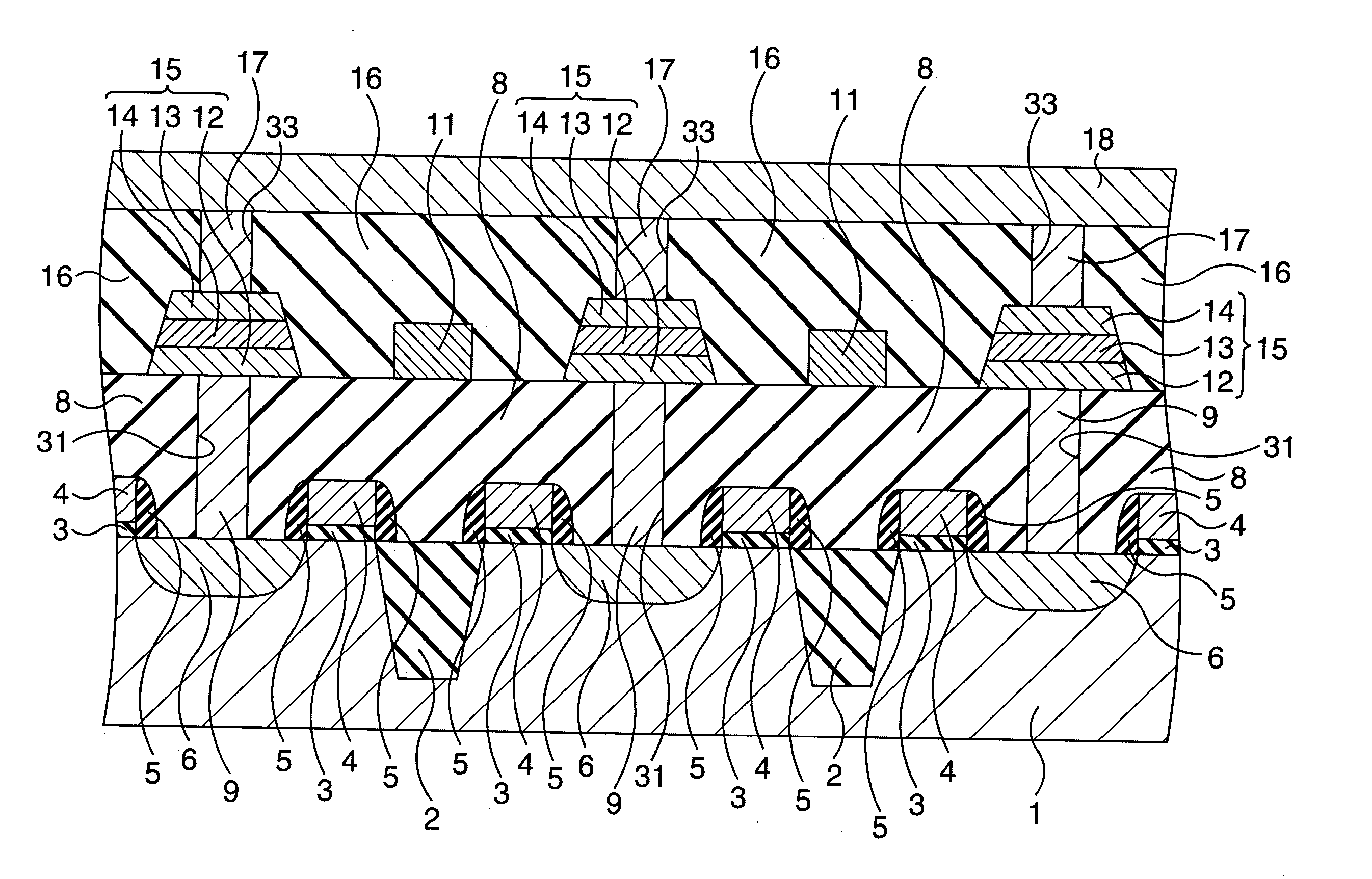
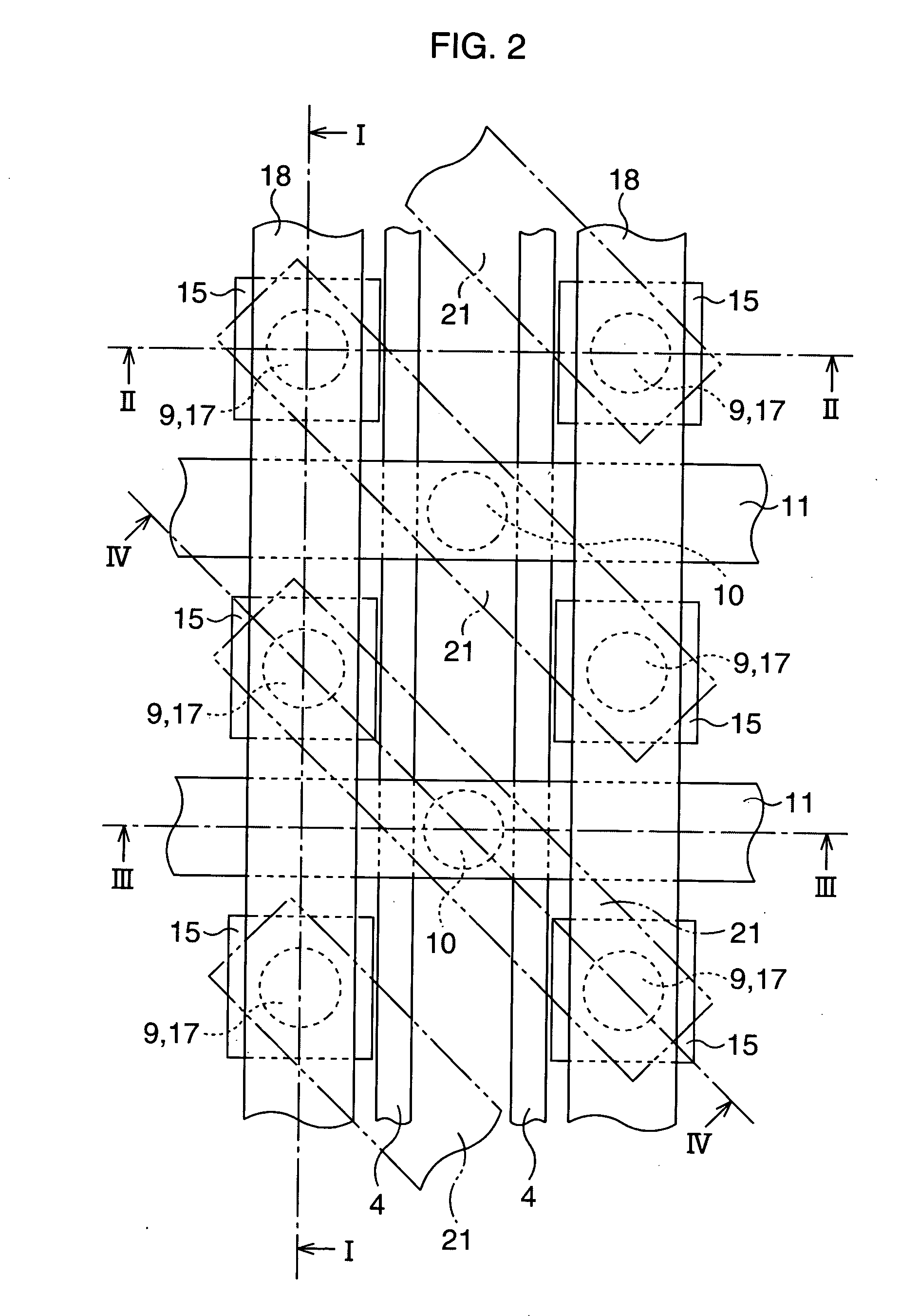
[0035] Hereinbelow, a first embodiment of the present invention will be described. FIG. 2 is a layout illustrating a configuration of a semiconductor device (ferroelectric memory) according to the first embodiment of the present invention. FIG. 3 is a sectional view taken along the I-I line in FIG. 2. FIG. 4A is a sectional view taken along the II-II line in FIG. 2. FIG. 4B is a sectional view taken along the III-III line in FIG. 2. FIG. 5 is a sectional view taken along the IV-IV line in FIG. 2.

[0036] In the present embodiment, as shown in FIG. 2 to FIG. 5, element isolation insulating films 2 for isolating a plurality of element regions 21 extending in one direction are formed for example by STI (Shallow Trench Isolation) method on the surface of a semiconductor substrate 1 such as a silicon substrate or the like. In addition, gate electrodes 4 (word lines) inclining at an angle of 45 degrees to the extending direction of the element regions 21 are formed via gate insulating film...

second embodiment

[0044] Subsequently, a second embodiment of the present invention will be described. FIG. 6 is a layout illustrating a configuration of a semiconductor device (ferroelectric memory) according to the second embodiment of the present invention. FIG. 7 is a sectional view taken along the I-I line in FIG. 6.

[0045] In the present embodiment, differently from the first embodiment, an element region 21 has a dogleg planar shape and the extending direction of a gate electrode 4 (word line) is parallel to a bit line 11 and orthogonal to a plate line 18. Two impurity diffused layers 6 provided in the same element region 21 are connected to lower electrodes 12 of ferroelectric capacitors 15 of which upper electrodes 14 are connected to the same plate line 18.

[0046] Also, in this second embodiment configured as described above, the same effects as of the first embodiment can be obtained.

third embodiment

[0047] Subsequently, a third embodiment of the present invention will be described. FIG. 8 is a layout illustrating a configuration of a semiconductor device (ferroelectric memory) according to the third embodiment of the present invention. In the present embodiment, a ferroelectric capacitor 15 has a circular planar shape in comparison with that of the prior layout shown in FIG. 10 to FIG. 12.

[0048] In the third embodiment as described above, in the manufacturing process thereof, deposits generally become difficult to adhere to the sidewall 5 of the ferroelectric capacitor 15 at the time of the high-temperature simultaneous etching, enabling to reduce leakage current. Whereas, the sidewall deposits have an advantage of preventing a capacitor insulating film 13 from damages as mentioned before. Preferably, therefore, in the high-temperature simultaneous etching, etching conditions are adjusted so that the damages of the capacitor insulating film 13 are prevented. At the time of the...


PUM


Abstract

There is formed a gate electrode (word line) via a gate insulating film on a semiconductor substrate, the gate electrode extending in the direction inclining at an angle of approximately 45 degrees to the extending direction of an element region. The element region is divided into three portions by the two gate electrodes. In each element region portion, two MOS transistors are provided. A bit line is connected to a W plug provided in the central region portion and lower electrodes of two ferroelectric capacitors are connected to other W plugs provided in both end region portions. The extending direction of the bit line inclines approximately 45 degrees to the extending direction of the element region.

Description

CROSS-REFERENCE TO RELATED APPLICATIONS [0001] This application is based upon and claims the benefit of priority from the prior Japanese Patent Application No. 2003-364917, filed on Oct. 24, 2003, the entire contents of which are incorporated herein by reference. BACKGROUND OF THE INVENTION [0002] [Field of the Invention][0003] The present invention relates to a semiconductor device suitable for a ferroelectric memory and a manufacturing method thereof. [Description of the Related Art][0004] Recently, with the purpose of improving integration, the shape having a practically vertical side surface is expected for a shape of a ferroelectric capacitor for example of the 0.18 μm generation. For this purpose, for example in a simultaneous etching at a high temperature using a hard mask, such a technique is beginning to be employed as etching simultaneously an upper electrode film, a ferroelectric film, and a lower electrode film. As a structure of the hard mask here, a lamination structu...

Claims


Application Information

Patent Timeline
Patent Type & Authority Applications(United States)
IPC IPC(8): H01L21/00H01L21/02H01L27/105H01L21/8246H01L27/115H01L29/76
CPCH01L27/11502H01L28/55H01L27/11507H10B53/30H10B53/00
Inventor ANDO, TAKASHI
Owner FUJITSU MICROELECTRONICS LTD
Why Eureka
Try Eureka