Method and structure of column interconnect

a column and interconnection technology, applied in the field of semiconductor devices, can solve the problems of brittle or soft materials, damage to low k dielectric materials, and easy damage to low k materials

Inactive Publication Date: 2002-12-17
VEECO INSTR
View PDF5 Cites 68 Cited by
  • Summary
  • Abstract
  • Description
  • Claims
  • Application Information

AI Technical Summary

Problems solved by technology

However, many low k materials are brittle or soft as compared to silicon dioxide and, when bonding forces are applied, the low k materials can be easily damaged.
More specifically, the forces applied during bonding processes (such as ultrasonic wirebonding) or during the formation of solderball (C4) connections, can damage the low k dielectric ma...

Method used


Image

  • Method and structure of column interconnect
  • Method and structure of column interconnect
  • Method and structure of column interconnect

Examples


first embodiment

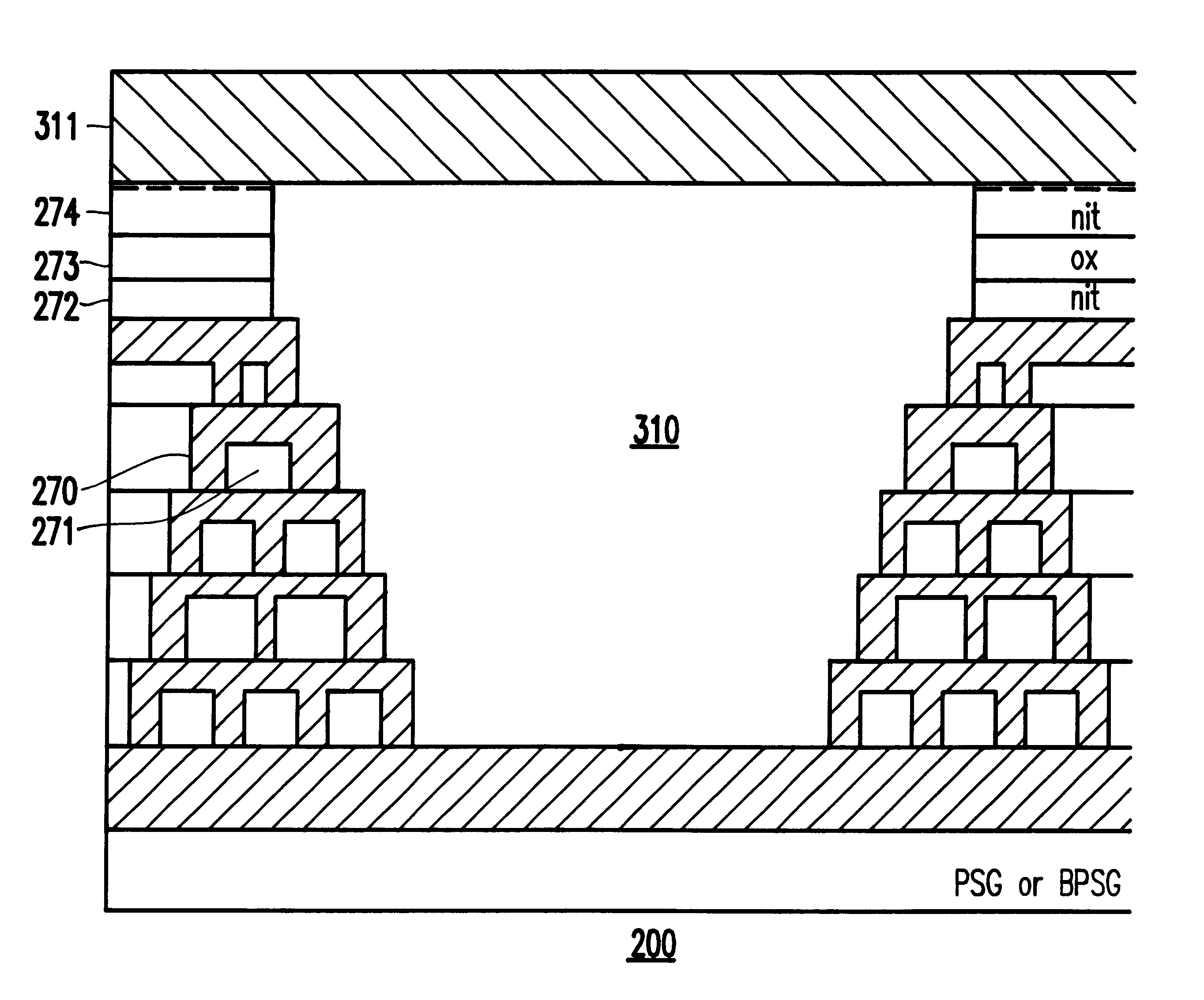
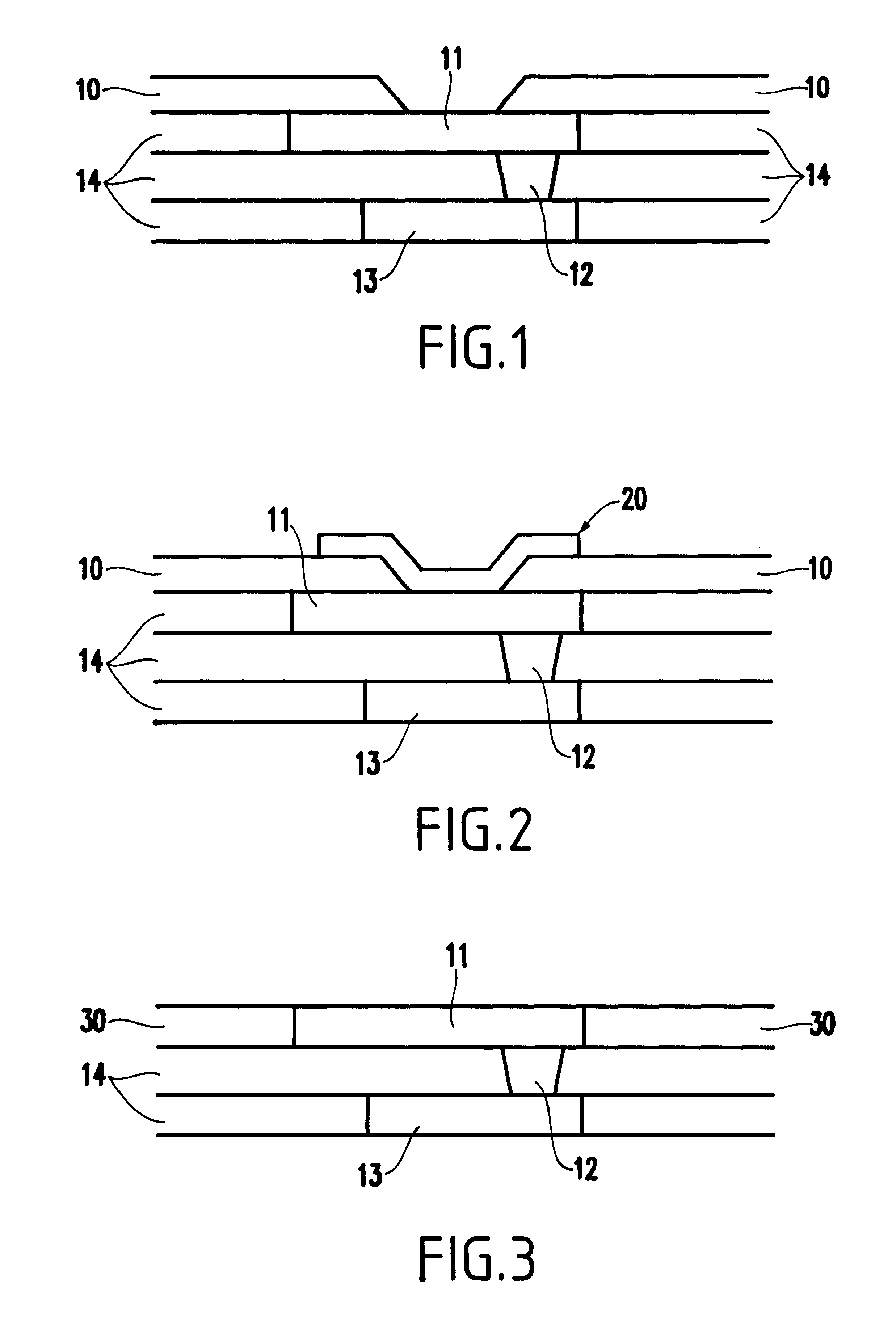
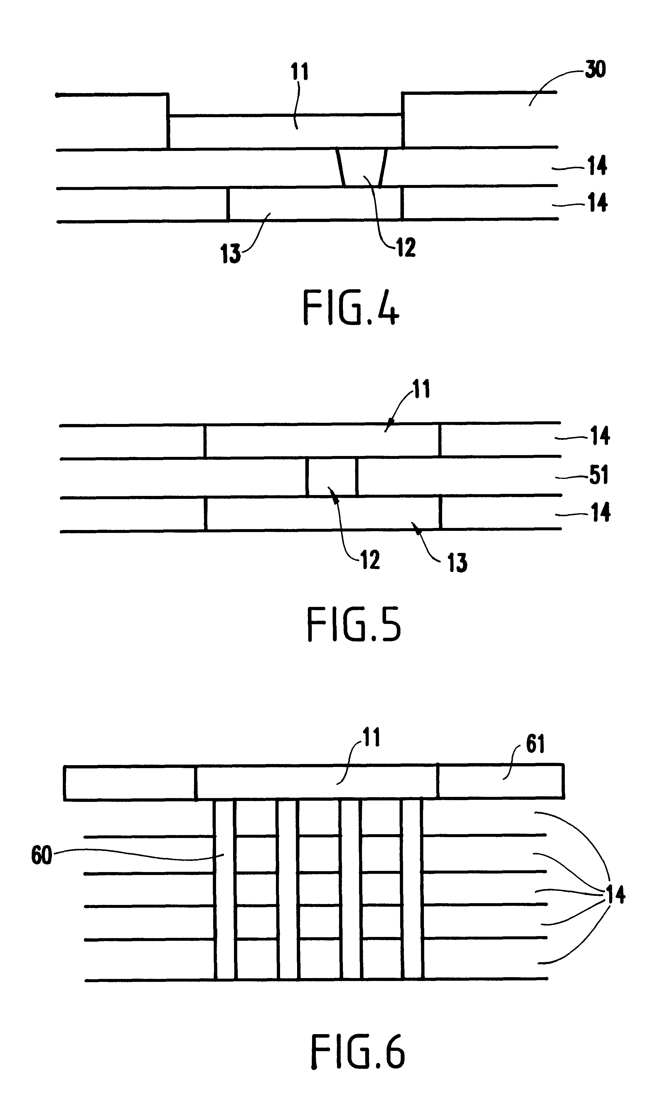
the invention is illustrated in FIG. 1 and includes a last metallization layer (LM) 11, a second to last metallization layer (LM-1) 13, a conductive via 12 connecting the two metallization layers 11, 13, and inter-layer dielectrics 14 which provide electrical insulation, but are too fragile to provide adequate mechanical support. In addition to the conventional structure, the invention includes a protective cap 10.

The invention adds the protective cap 10 above the last metallization (LM) layer 11. The thickness of the cap 10 is between 1 and 20 microns, and is preferably 10 microns thick. The cap 10 can be formed of, for example, silicon dioxide (SiO.sub.2), (spin-on-glass) SOG, silicon nitride, doped SiO.sub.2 (i.e. F, B, P), HSQ, MSQ or other similar protective substance. The preferred embodiment would comprise 50 .mu.m nitride, 1 .mu.m oxide, 1 .mu.m nitride, 1 .mu.m oxide (nitride=Si.sub.x N.sub.y H.sub.z an oxide=SiO.sub.2), but could be any similar structure. Note the initial ...


PUM


Abstract

A method and structure for a semiconductor chip includes a plurality of layers of interconnect metallurgy, at least one layer of deformable dielectric material over the interconnect metallurgy, at least one input/output bonding pad, and a support structure that includes a substantially rigid dielectric in a supporting relationship to the pad that avoids crushing the deformable dielectric material.

Description

1. Field of the InventionThe present invention generally relates to semiconductor chips and more particularly to structures which protect the chip during bonding processes.2. Description of the Related ArtThe use of low dielectric potential (k) interlevel dielectric (ILD) materials (e.g., spin-on-glass (SOG), Hydrogensilsesquioxane(HSQ), Methylisilane (MSQ), Benzocyclobutene (BCB), etc.) has become very popular for input / output (UO) and mechanical support structures which are applied to a previously fabricated semiconductor chip. Such I / O and support structures are formed after the logical function sections of the semiconductor chip have been completed. Therefore, such structures / processing are sometimes referred to as "back end of line" (BEOL) structures / processing because they are formed at the back end of the production line.However, many low k materials are brittle or soft as compared to silicon dioxide and, when bonding forces are applied, the low k materials can be easily dama...

Claims


Application Information

Patent Timeline
IPC IPC(8): H01L23/532H01L21/02H01L23/485H01L21/70H01L23/31H01L21/768H01L21/60H01L23/28H01L23/48H01L23/52H01L21/3205
CPCH01L21/76801H01L23/3171H01L23/5329H01L24/03H01L24/05H01L24/11H01L24/12H01L2924/0002H01L2224/05006H01L2224/05556H01L2224/05567H01L2224/05624H01L2224/13022H01L2224/13099H01L2224/45124H01L2224/45144H01L2924/01004H01L2924/01005H01L2924/01006H01L2924/01013H01L2924/01014H01L2924/01015H01L2924/01022H01L2924/01027H01L2924/01029H01L2924/01033H01L2924/01039H01L2924/0105H01L2924/01073H01L2924/01074H01L2924/01079H01L2924/01082H01L2924/01327H01L2924/014H01L2924/04953H01L2924/05042H01L2924/14H01L21/76835H01L2224/04042H01L2224/0401H01L2224/48724H01L2224/48624H01L2924/01019H01L24/45H01L2924/00014H01L2924/00H01L2224/05552H01L21/60
Inventor ELLIS-MONAGHAN, JOHN J.FEENEY, PAUL M.GEFFKEN, ROBERT M.LANDIS, HOWARD S.PREVITI-KELLY, ROSEMARY A.BERGMAN REUTER, BETTE L.RUTTEN, MATTHEW J.STAMPER, ANTHONY K.YANKEE, SALLY J.
Owner VEECO INSTR
Why Eureka
Try Eureka